The transistor amplifier, despite its long history, remains a favorite subject of research for both beginners and seasoned radio amateurs. And this is understandable. It is an indispensable component of the most popular low (sound) frequency amplifiers. We will look at how simple transistor amplifiers are built.
Amplifier frequency response
In any television or radio receiver, in every music center or sound amplifier you can find transistor sound amplifiers (low frequency - LF). The difference between transistor audio amplifiers and other types lies in their frequency characteristics.
A transistor-based audio amplifier has a uniform frequency response in the frequency band from 15 Hz to 20 kHz. This means that the amplifier converts (amplify) all input signals with a frequency within this range approximately equally. The figure below shows the ideal frequency response curve for an audio amplifier in the coordinates “amplifier gain Ku - input signal frequency.”
This curve is almost flat from 15 Hz to 20 kHz. This means that such an amplifier should be used specifically for input signals with frequencies between 15 Hz and 20 kHz. For input signals with frequencies above 20 kHz or below 15 Hz, its efficiency and performance degrade quickly.
The type of frequency response of the amplifier is determined by the electrical radio elements (ERE) of its circuit, and primarily by the transistors themselves. A transistor-based audio amplifier is usually assembled using so-called low- and mid-frequency transistors with a total input signal bandwidth from tens and hundreds of Hz to 30 kHz.
Amplifier operating class
As is known, depending on the degree of continuity of current flow throughout its period through a transistor amplification stage (amplifier), the following classes of its operation are distinguished: “A”, “B”, “AB”, “C”, “D”.
In operating class, current “A” flows through the cascade for 100% of the input signal period. The operation of the cascade in this class is illustrated by the following figure.

In the operating class of the amplifier stage "AB", current flows through it for more than 50%, but less than 100% of the input signal period (see figure below).

In the "B" stage operation class, the current flows through it for exactly 50% of the input signal period, as illustrated in the figure.

Finally, in class C stage operation, current flows through it for less than 50% of the input signal period.
Low-frequency amplifier using transistors: distortion in the main classes of operation
In the working area, a class “A” transistor amplifier has a low level of nonlinear distortion. But if the signal has pulsed voltage surges, leading to saturation of the transistors, then higher harmonics (up to the 11th) appear around each “standard” harmonic of the output signal. This causes the phenomenon of so-called transistor, or metallic, sound.
If low-frequency power amplifiers using transistors have an unstabilized power supply, then their output signals are amplitude modulated near the mains frequency. This leads to a harsh sound at the left end of the frequency response. Various methods of voltage stabilization make the amplifier design more complex.
The typical efficiency of a single-ended class A amplifier does not exceed 20% due to the constantly open transistor and the continuous flow of a constant current component. You can make a class A amplifier push-pull, the efficiency will increase slightly, but the half-waves of the signal will become more asymmetrical. Transferring a cascade from operating class “A” to operating class “AB” quadruples nonlinear distortions, although the efficiency of its circuit increases.
In class “AB” and “B” amplifiers, distortion increases as the signal level decreases. One involuntarily wants to turn up such an amplifier louder to fully experience the power and dynamics of the music, but often this does not help much.
Intermediate grades of work
Work class "A" has a variation - class "A+". In this case, the low-voltage input transistors of an amplifier of this class operate in class “A”, and the high-voltage output transistors of the amplifier, when their input signals exceed a certain level, go into classes “B” or “AB”. The efficiency of such cascades is better than in pure class “A”, and nonlinear distortions are less (up to 0.003%). However, they also have a “metallic” sound due to the presence of higher harmonics in the output signal.
In amplifiers of another class - "AA" the degree of nonlinear distortion is even lower - about 0.0005%, but higher harmonics are also present.
Return to the Class A transistor amplifier?
Today, many experts in the field of high-quality sound reproduction advocate a return to tube amplifiers, since the level of nonlinear distortions and higher harmonics they introduce into the output signal is obviously lower than that of transistors. However, these advantages are largely offset by the need for a matching transformer between the high-impedance tube output stage and low-impedance audio speakers. However, a simple transistor amplifier can be made with a transformer output, as will be shown below.
There is also a point of view that the ultimate sound quality can only be provided by a hybrid tube-transistor amplifier, all stages of which are single-ended, not covered and operate in class “A”. That is, such a power repeater is an amplifier with a single transistor. Its circuit can have a maximum achievable efficiency (in class “A”) of no more than 50%. But neither the power nor the efficiency of the amplifier are indicators of the quality of sound reproduction. In this case, the quality and linearity of the characteristics of all ERE in the circuit acquire special importance.
Since single-ended circuits are gaining this perspective, we will look at their possible variations below.
Single-ended amplifier with one transistor
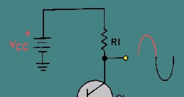
Its circuit, made with a common emitter and R-C connections for input and output signals for operation in class “A”, is shown in the figure below.

It shows transistor Q1 of the n-p-n structure. Its collector is connected to the positive terminal +Vcc through current-limiting resistor R3, and the emitter is connected to -Vcc. An amplifier based on a pnp structure transistor will have the same circuit, but the power supply terminals will change places.
C1 is a decoupling capacitor by which the AC input signal source is separated from the DC voltage source Vcc. In this case, C1 does not prevent the passage of alternating input current through the base-emitter junction of transistor Q1. Resistors R1 and R2, together with the resistance of the E - B junction, form Vcc to select the operating point of transistor Q1 in static mode. A typical value for this circuit is R2 = 1 kOhm, and the position of the operating point is Vcc/2. R3 is a load resistor of the collector circuit and serves to create an alternating voltage output signal on the collector.
Let us assume that Vcc = 20 V, R2 = 1 kOhm, and the current gain h = 150. We select the voltage at the emitter Ve = 9 V, and the voltage drop across the “E - B” junction is taken equal to Vbe = 0.7 V. This value corresponds to the so-called silicon transistor. If we were considering an amplifier based on germanium transistors, then the voltage drop across the open junction “E - B” would be equal to Vbe = 0.3 V.
Emitter current approximately equal to collector current
Ie = 9 V/1 kOhm = 9 mA ≈ Ic.
Base current Ib = Ic/h = 9 mA/150 = 60 µA.
Voltage drop across resistor R1
V(R1) = Vcc - Vb = Vcc - (Vbe + Ve) = 20 V - 9.7 V = 10.3 V,
R1 = V(R1)/Ib = 10.3 V/60 µA = 172 kOhm.
C2 is needed to create a circuit for passing the alternating component of the emitter current (actually the collector current). If it were not there, then resistor R2 would greatly limit the variable component, so that the bipolar transistor amplifier in question would have a low current gain.
In our calculations, we assumed that Ic = Ib h, where Ib is the base current flowing into it from the emitter and arising when a bias voltage is applied to the base. However, a leakage current from the collector Icb0 always flows through the base (both with and without bias). Therefore, the real collector current is equal to Ic = Ib h + Icb0 h, i.e. The leakage current in a circuit with OE is amplified by 150 times. If we were considering an amplifier based on germanium transistors, then this circumstance would need to be taken into account in the calculations. The fact is that they have a significant Icb0 of the order of several μA. For silicon, it is three orders of magnitude smaller (about several nA), so it is usually neglected in calculations.
Single-ended amplifier with MOS transistor
Like any field-effect transistor amplifier, the circuit under consideration has its analogue among amplifiers. Therefore, let’s consider an analogue of the previous circuit with a common emitter. It is made with a common source and R-C connections for input and output signals for operation in class “A” and is shown in the figure below.

Here C1 is the same decoupling capacitor, through which the AC input signal source is separated from the DC voltage source Vdd. As you know, any amplifier based on field-effect transistors must have the gate potential of its MOS transistors lower than the potentials of their sources. In this circuit, the gate is grounded by resistor R1, which usually has a high resistance (from 100 kOhm to 1 Mohm) so that it does not shunt the input signal. There is practically no current passing through R1, so the gate potential in the absence of an input signal is equal to the ground potential. The source potential is higher than the ground potential due to the voltage drop across resistor R2. Thus, the gate potential is lower than the source potential, which is necessary for normal operation of Q1. Capacitor C2 and resistor R3 have the same purpose as in the previous circuit. Since this is a common source circuit, the input and output signals are 180° out of phase.
Amplifier with transformer output
The third single-stage simple transistor amplifier, shown in the figure below, is also made according to a common-emitter circuit for operation in class "A", but it is connected to a low-impedance speaker through a matching transformer.

The primary winding of transformer T1 loads the collector circuit of transistor Q1 and develops the output signal. T1 transmits the output signal to the speaker and matches the transistor's output impedance to the low (on the order of a few ohms) impedance of the speaker.
The voltage divider of the collector power supply Vcc, assembled on resistors R1 and R3, ensures the selection of the operating point of transistor Q1 (supplying a bias voltage to its base). The purpose of the remaining elements of the amplifier is the same as in the previous circuits.
Push-pull audio amplifier
A push-pull LF amplifier with two transistors splits the input frequency into two antiphase half-waves, each of which is amplified by its own transistor stage. After performing such amplification, the half-waves are combined into a complete harmonic signal, which is transmitted to the speaker system. Such a transformation of the low-frequency signal (splitting and re-merging), naturally, causes irreversible distortion in it, due to the difference in the frequency and dynamic properties of the two transistors of the circuit. These distortions reduce the sound quality at the amplifier output.
Push-pull amplifiers operating in class “A” do not reproduce complex audio signals well enough, since a direct current of increased magnitude continuously flows in their arms. This leads to asymmetry of signal half-waves, phase distortion and ultimately loss of sound intelligibility. When heated, two powerful transistors double the signal distortion in the low and infra-low frequencies. But still, the main advantage of the push-pull circuit is its acceptable efficiency and increased output power.
A push-pull circuit of a power amplifier using transistors is shown in the figure.

This is an amplifier for operation in class “A”, but class “AB” and even “B” can be used.
Transformerless transistor power amplifier
Transformers, despite the successes in their miniaturization, still remain the most bulky, heaviest and most expensive electronic devices. Therefore, a way was found to eliminate the transformer from the push-pull circuit by performing it on two powerful complementary transistors of different types (n-p-n and p-n-p). Most modern power amplifiers use precisely this principle and are designed to operate in class "B". The circuit of such a power amplifier is shown in the figure below.

Both of its transistors are connected according to a circuit with a common collector (emitter follower). Therefore, the circuit transfers the input voltage to the output without amplification. If there is no input signal, then both transistors are on the border of the on state, but they are turned off.
When a harmonic signal is applied to the input, its positive half-wave opens TR1, but puts the pnp transistor TR2 completely in cutoff mode. Thus, only the positive half-wave of the amplified current flows through the load. The negative half-wave of the input signal opens only TR2 and closes TR1, so that the negative half-wave of the amplified current is supplied to the load. As a result, a full power-amplified (due to current amplification) sinusoidal signal is released at the load.
Single transistor amplifier
To understand the above, let’s assemble a simple amplifier using transistors with our own hands and figure out how it works.
As a load for a low-power transistor T of type BC107, we will turn on headphones with a resistance of 2-3 kOhm, apply a bias voltage to the base from a high-resistance resistor R* of 1 MOhm, and connect a decoupling electrolytic capacitor C with a capacity of 10 μF to 100 μF into the base circuit T. Power the circuit We will use 4.5 V/0.3 A from the battery.

If resistor R* is not connected, then there is neither base current Ib nor collector current Ic. If a resistor is connected, the voltage at the base rises to 0.7 V and a current Ib = 4 μA flows through it. The current gain of the transistor is 250, which gives Ic = 250Ib = 1 mA.
Having assembled a simple transistor amplifier with our own hands, we can now test it. Connect the headphones and place your finger on point 1 of the diagram. You will hear a noise. Your body perceives power supply radiation at a frequency of 50 Hz. The noise you hear from your headphones is this radiation, only amplified by a transistor. Let us explain this process in more detail. A 50 Hz AC voltage is connected to the base of the transistor through capacitor C. The base voltage is now equal to the sum of the DC offset voltage (approximately 0.7 V) coming from resistor R* and the AC finger voltage. As a result, the collector current receives an alternating component with a frequency of 50 Hz. This alternating current is used to shift the speaker membrane back and forth at the same frequency, meaning that we will be able to hear a 50Hz tone at the output.
Listening to a noise level of 50 Hz is not very interesting, so you can connect low-frequency signal sources (CD player or microphone) to points 1 and 2 and hear amplified speech or music.
After mastering the basics of electronics, the novice radio amateur is ready to solder his first electronic designs. Audio power amplifiers are typically the most repeatable designs. There are quite a lot of schemes, each with its own parameters and design. This article will discuss several simple and fully working amplifier circuits that can be successfully repeated by any radio amateur. The article does not use complex terms and calculations; everything is simplified as much as possible so that no additional questions arise.
Let's start with a more powerful circuit.
So, the first circuit is made on the well-known TDA2003 microcircuit. This is a mono amplifier with an output power of up to 7 watts into a 4 ohm load. I want to say that the standard circuit for connecting this microcircuit contains a small number of components, but a couple of years ago I came up with a different circuit on this microcircuit. In this circuit, the number of components is reduced to a minimum, but the amplifier has not lost its sound parameters. After developing this circuit, I began making all my amplifiers for low-power speakers using this circuit.
The circuit of the presented amplifier has a wide range of reproducible frequencies, a supply voltage range from 4.5 to 18 volts (typical 12-14 volts). The microcircuit is installed on a small heat sink, since the maximum power reaches up to 10 Watts.
The microcircuit is capable of operating at a load of 2 ohms, which means that 2 heads with a resistance of 4 ohms can be connected to the amplifier output.
The input capacitor can be replaced with any other one, with a capacity from 0.01 to 4.7 μF (preferably from 0.1 to 0.47 μF), you can use both film and ceramic capacitors. It is advisable not to replace all other components.

Volume control from 10 to 47 kOhm.
The output power of the microcircuit allows it to be used in low-power speakers for PCs. It is very convenient to use the chip for stand-alone speakers for a mobile phone, etc.
The amplifier works immediately after switching on and does not require additional adjustment. It is recommended to additionally connect the power supply minus to the heat sink. It is advisable to use all electrolytic capacitors at 25 Volts.
The second circuit is assembled using low-power transistors and is more suitable as a headphone amplifier.

This is probably the highest quality circuit of its kind, the sound is clear, you can feel the entire frequency spectrum. With good headphones, it feels like you have a full-fledged subwoofer.

The amplifier is assembled with only 3 reverse conduction transistors; as the cheapest option, transistors of the KT315 series were used, but their choice is quite wide.
The amplifier can operate at a low-impedance load, up to 4 ohms, which makes it possible to use the circuit to amplify the signal of a player, radio, etc. A 9-volt Krona battery is used as a power source.
The final stage also uses KT315 transistors. To increase the output power, you can use KT815 transistors, but then you will have to increase the supply voltage to 12 volts. In this case, the amplifier power will reach up to 1 Watt. The output capacitor can have a capacity from 220 to 2200 µF.
The transistors in this circuit do not heat up, therefore, no cooling is needed. If you use larger output transistors, you may need small heat sinks for each transistor.
And finally - the third scheme. An equally simple, but proven version of the amplifier structure is presented. The amplifier is capable of operating from reduced voltage to 5 volts, in which case the PA output power will be no more than 0.5 W, and the maximum power with a 12 volt supply reaches up to 2 Watts.

The output stage of the amplifier is built on a domestic complementary pair. The amplifier is regulated by selecting resistor R2. To do this, it is advisable to use a 1 kOhm trimmer. Slowly rotate the regulator until the quiescent current of the output stage is 2-5 mA.
The amplifier does not have high input sensitivity, so it is advisable to use a pre-amplifier before the input.

The diode plays a significant role in the circuit; it is here to stabilize the mode of the output stage.
The output stage transistors can be replaced with any complementary pair of corresponding parameters, for example KT816/817. The amplifier can power low-power stand-alone speakers with a load resistance of 6-8 ohms.
List of radioelements
| Designation | Type | Denomination | Quantity | Note | Shop | My notepad | |
|---|---|---|---|---|---|---|---|
| Amplifier on TDA2003 chip | |||||||
| Audio amplifier | TDA2003 | 1 | To notepad | ||||
| C1 | 47 uF x 25V | 1 | To notepad | ||||
| C2 | Capacitor | 100 nF | 1 | Film | To notepad | ||
| C3 | Electrolytic capacitor | 1 uF x 25V | 1 | To notepad | |||
| C5 | Electrolytic capacitor | 470 uF x 16V | 1 | To notepad | |||
| R1 | Resistor | 100 Ohm | 1 | To notepad | |||
| R2 | Variable resistor | 50 kOhm | 1 | From 10 kOhm to 50 kOhm | To notepad | ||
| Ls1 | Dynamic head | 2-4 Ohm | 1 | To notepad | |||
| Transistor amplifier circuit No. 2 | |||||||
| VT1-VT3 | Bipolar transistor | KT315A | 3 | To notepad | |||
| C1 | Electrolytic capacitor | 1 uF x 16V | 1 | To notepad | |||
| C2, C3 | Electrolytic capacitor | 1000 uF x 16V | 2 | To notepad | |||
| R1, R2 | Resistor | 100 kOhm | 2 | To notepad | |||
| R3 | Resistor | 47 kOhm | 1 | To notepad | |||
| R4 | Resistor | 1 kOhm | 1 | To notepad | |||
| R5 | Variable resistor | 50 kOhm | 1 | To notepad | |||
| R6 | Resistor | 3 kOhm | 1 | To notepad | |||
| Dynamic head | 2-4 Ohm | 1 | To notepad | ||||
| Transistor amplifier circuit No. 3 | |||||||
| VT2 | Bipolar transistor | KT315A | 1 | To notepad | |||
| VT3 | Bipolar transistor | KT361A | 1 | To notepad | |||
| VT4 | Bipolar transistor | KT815A | 1 | To notepad | |||
| VT5 | Bipolar transistor | KT816A | 1 | To notepad | |||
| VD1 | Diode | D18 | 1 | Or any low power | To notepad | ||
| C1, C2, C5 | Electrolytic capacitor | 10 uF x 16V | 3 | ||||
I would like to present the design of a simple but powerful low-frequency amplifier, made using modern inexpensive transistors. The main advantages of this amplifier are ease of assembly, accessible and cheap radio components, and the finished amplifier does not require adjustment and works immediately. The amplifier develops very high power compared to similar circuits. Among the electrical parameters, I would like to note the very high linearity in the operating frequency range from 20Hz to 20kHz. True, it was not without its shortcomings either. This circuit has an increased noise level at high volumes, but if you take into account the simplicity and accessibility, it is still worth assembling an amplifier, I especially advise car enthusiasts for a powerful subwoofer, since the power of such a circuit is quite sufficient to drive high-power imported heads. From the diagram it is clear that it couldn’t be simpler. The circuit uses only 5 transistors and several additional radio components.
To reduce the noise level of the amplifier, you will need to install a variable resistor at the input with a resistance of 20 to 100 kOhm; they will also control the volume. In this case, at low volume there will be practically no noise, and at high volume we hardly hear the noise, and if the amplifier operates with a low-pass filter at the input (under the subwoofer), then there will be no noise at all.

The amplifier is capable of delivering about 100 watts into an 8 ohm load! if a head with a resistance of 4 ohms is used, then the power increases to 150 watts! UMZCH parameters:
Voltage gain................................................................. ........20
Supply voltage Up................................................................... ................................+-15…+-50V
Rated power P at Upit = +-30V at 4 Ohm.................................................... ....100W
Maximum power Pmax Upit=+-45V at 4 Ohm.................................... ..150W
Input sensitivity Uin.................................................... ...........................1B
Total coefficient of all types of distortion at P=60W 4Ohm, Kd........................0.005%
Amplifier quiescent current Ixx.................................................... ....................................20-25mA
Quiescent current of the output stage.................................................... ........................0mA
Reproducible frequency band at –3dB level, Hz,................................5-100,000

The parameters are quite good, the only obstacle to using the circuit as a car amplifier is the increased bipolar power supply, but this is not such a big obstacle, since many voltage converter circuits are known today, one of such circuits is based on the TL494 chip. The circuit is standard and allows you to get up to 200 watts of power at the transformer output, which is quite enough for the full operation of this homemade amplifier. I don’t show the converter circuit, since this is a completely different topic.
I would like to offer novice lovers of high-quality sound reproduction one of the developed and tested ULF circuits. This design will help make a high-quality amplifier that can be modified at minimal cost and the amplifier can be used for researching circuit designs.
This will help you on your way from simple to complex and more perfect. Attached to the description are files of printed circuit boards that can be transformed to fit a specific case.
In the presented version, the housing from Radiotekhnika U-101 was used.
I developed and made this power amplifier in the last century from what could be purchased without difficulty. I wanted to make a design with the highest possible price-quality ratio. This is not High-End, but not third grade either. The amplifier has high-quality sound, excellent repeatability and is easy to set up.
Amplifier circuit diagram
The circuit is completely symmetrical for the positive and negative half-waves of the low-frequency signal. The input stage is made using transistors VT1 – VT4. It differs from the prototype in transistors VT1 and VT4, which increase the linearity of the stages on transistors VT2 and VT3. There are many circuit types of input stages with various advantages and disadvantages. This cascade was chosen because of its simplicity and the possibility of reducing the nonlinearity of the amplitude characteristics of transistors. With the advent of more advanced input stage circuits, it can be replaced.The negative feedback signal (NFS) is taken from the output of the voltage amplifier and enters the emitter circuits of transistors VT2 and VT3. The rejection of general OOS is due to the desire to get rid of the influence on OOS of all unnecessary things that are not the output signal of the circuit. This has its pros and cons. With this configuration this is justified. With higher quality components, you can try with different types of feedback.
A cascode circuit was chosen as a voltage amplifier, which has a high input resistance, low pass-through capacitance and lower nonlinear distortions in comparison with the OE circuit. The disadvantage of the cascode circuit is the lower amplitude of the output signal. This is the price to pay for less distortion. If you install jumpers, you can also assemble an OE circuit on a printed circuit board. Powering the voltage amplifier from a separate voltage source was not introduced due to the desire to simplify the design of the ULF.
The output stage is a parallel amplifier, which has a number of advantages over other circuits. One of the important advantages is the linearity of the circuit with a significant spread in the parameters of the transistors, which was checked when assembling the amplifier. This cascade should perhaps have greater linearity, because there is no overall OOS and the quality of the amplifier’s output signal greatly depends on it. Amplifier supply voltage 30 V.
Amplifier design
I developed printed circuit boards for “affordable” cases from Radiotekhnika U-101 amplifiers. The circuit was placed on two parts of the printed circuit board. The first part, which is fixed to the radiator, houses a “parallel” amplifier and a voltage amplifier. The second part of the board houses the input stage. This board is attached to the first board using corners. This division of the board into two parts allows the amplifier to be improved with minimal design changes. In addition, this arrangement can also be used for laboratory studies of cascades.The amplifier must be assembled in several stages. Assembly begins with a parallel amplifier and its setup. In the second stage, the rest of the circuit is assembled and adjusted and the final minimization of circuit distortions is carried out. When placing the transistors of the output stage on the radiator, it is necessary to remember the need for thermal contact between the housings of transistors VT9, VT14 and VT10, VT13 in pairs.
Printed circuit boards were developed using the Sprint Layout 6 program, which will allow you to adjust the placement of elements on the board, i.e. customized for a specific configuration or case. See archives below.

Amplifier parts
The parameters of the amplifier depend on the quality of the radio elements used and their location on the board. The applied circuit solutions make it possible to do without selecting transistors, but it is advisable to use transistors with a cut-off amplification frequency from 5 to 200 MHz and a margin of maximum operating voltage of more than 2 times in comparison with the cascade supply voltage.If there is a desire and opportunity, then it is advisable to choose transistors according to the principle of “complementarity” and identical amplification characteristics. We tried manufacturing options with and without selecting transistors. The version with selected “complementary” domestic transistors showed significantly better performance than without selection. Only KT940 and KT9115 of the domestic transistors are complementary, while the rest have conditional complementarity. There are a lot of complementary pairs among foreign transistors, and information about this can be found on manufacturers’ websites and in reference books.
As VT1, VT3, VT5 it is possible to use transistors of the KT3107 series with any letters. As VT2, VT4, VT6 it is possible to use transistors of the KT3102 series with letters that have characteristics similar to the transistors used for another half-wave of the audio signal. If it is possible to select transistors according to parameters, then it is better to do so. Almost all modern testers allow you to do this without problems. With large deviations, the time spent on setting up will be greater and the result will be more modest. Transistors KT9115A, KP960A are suitable for VT6, and KT940A, KP959A are suitable for VT7.
Transistors KT817V (G), KT850A can be used as VT9 and VT12, and KT816V (G), KT851A can be used as VT10 and VT11. For VT13, transistors KT818V (G), KP964A are suitable, and for VT14 - KT819V (G), KP954A. Instead of zener diodes VD3 and VD4, you can use two AL307 LEDs connected in series or the like.
The circuit allows the use of other parts, but correction of the printed circuit boards may be required. Capacitor C1 can have a capacity from 1 µF to 4.7 µF and must be made of polypropylene or another, but of high quality. You can find information about this on amateur radio websites. The supply voltage, input and output signals are connected using printed circuit terminals.
Setting up the amplifier
When turned on for the first time, the ULF should be connected through powerful ceramic resistors (10 - 100 Ohms). This will save the elements from overloads and failure due to an installation error. On the first part of the board, resistor R23 sets the quiescent current ULF (150-250 mA) when the load is off. Next, you need to establish that there is no constant voltage at the output of the amplifier when an equivalent load is connected. This is done by changing the value of one of the resistors R19 or R20.After installing the rest of the circuit, set resistor R14 to the middle position. Using the load equivalent, the absence of excitation of the amplifier is checked and resistor R5 is used to establish the absence of constant voltage at the output of the amplifier. The amplifier can be considered configured in static mode.
To set up in dynamic mode, a serial RC circuit is connected in parallel to the load equivalent. Resistor with a power of 0.125 W and a nominal value of 1.3-4.7 kOhm. Non-polar capacitor 1-2 µF. We connect a microammeter (20-100 µA) in parallel to the capacitor. Then, by applying a sinusoidal signal with a frequency of 5-8 kHz to the amplifier input, you need to estimate the threshold saturation level of the amplifier using an oscilloscope and an AC voltmeter connected to the output. After this, we reduce the input signal to a level of 0.7 from saturation and use resistor R14 to achieve a minimum reading of the microammeter. In some cases, to reduce distortion at high frequencies, it is necessary to carry out phase correction in advance by installing capacitor C12 (0.02-0.033 μF).
Capacitors C8 and C9 are selected for the best transmission of a pulse signal with a frequency of 20 kHz (installed if necessary). Capacitor C10 can be omitted if the circuit is stable. By changing the value of resistor R15, the same gain is established for each of the channels of the stereo or multi-channel version. By changing the value of the quiescent current of the output stage, you can try to find the most linear operating mode.
Sound rating
The assembled amplifier has a very good sound. Listening to the amplifier for a long time does not lead to fatigue. Of course, there are better amplifiers, but in terms of the ratio of costs and resulting quality, many will like the circuit. With better quality parts and their selection, even more significant results can be achieved.Links and files
1. Korol V., “UMZCH with compensation for nonlinearity of the amplitude characteristic” - Radio, 1989, No. 12, p. 52-54.06/09/2017 - The scheme has been corrected, all archives have been re-uploaded.
▼
🕗 09/06/17 ⚖️ 24.43 Kb ⇣ 17
Hello, reader! My name is Igor, I'm 45, I'm a Siberian and an avid amateur electronics engineer. I came up with, created and have been maintaining this wonderful site since 2006.
For more than 10 years, our magazine has existed only at my expense.
Good! The freebie is over. If you want files and useful articles, help me!
Scheme No. 1
Selecting an amplifier class . Let us immediately warn the radio amateur - we will not make a class A amplifier using transistors. The reason is simple - as stated in the introduction, the transistor amplifies not only the useful signal, but also the bias applied to it. Simply put, it amplifies direct current. This current, together with the useful signal, will flow through the acoustic system (AS), and speakers, unfortunately, are able to reproduce this direct current. They do this in the most obvious way - by pushing or pulling the diffuser from its normal position to an unnatural one.
Try to press the speaker cone with your finger - and you will see what a nightmare the sound produced will turn into. Direct current in its action successfully replaces your fingers, so it is absolutely contraindicated for a dynamic head. You can separate direct current from an alternating signal by only two means - a transformer or a capacitor - and both options, as they say, are worse than the other.
Schematic diagram
The circuit of the first amplifier that we will assemble is shown in Fig. 11.18.
This is a feedback amplifier, the output stage of which operates in mode B. The only advantage of this circuit is its simplicity, as well as the uniformity of the output transistors (no special complementary pairs are required). However, it is quite widely used in low-power amplifiers. Another advantage of the scheme is that it does not require any configuration, and if the parts are in good working order, it will work immediately, and this is very important for us now.
Let's consider the operation of this circuit. The amplified signal is supplied to the base of transistor VT1. The signal amplified by this transistor from resistor R4 is supplied to the base of the composite transistor VT2, VT4, and from it to resistor R5.
Transistor VT3 is turned on in emitter follower mode. It amplifies the positive half-waves of the signal on resistor R5 and supplies them through capacitor C4 to the speaker.
The negative half-waves are enhanced by the composite transistor VT2, VT4. In this case, the voltage drop across diode VD1 closes transistor VT3. The signal from the amplifier output is fed to the feedback circuit divider R3, R6, and from it to the emitter of the input transistor VT1. Thus, transistor VT1 plays the role of a comparison device in the feedback circuit.
It amplifies direct current with a gain equal to unity (because the resistance of capacitor C to direct current is theoretically infinite), and the useful signal with a gain equal to the ratio R6/R3.
As you can see, the capacitance value of the capacitor is not taken into account in this formula. The frequency from which the capacitor can be neglected in calculations is called the cutoff frequency of the RC circuit. This frequency can be calculated using the formula
F = 1 / (R×C).
For our example, it will be about 18 Hz, i.e. the amplifier will amplify lower frequencies worse than it could.
Pay . The amplifier is assembled on a board made of single-sided fiberglass 1.5 mm thick with dimensions 45×32.5 mm. The PCB layout in a mirror image and the parts layout can be downloaded. You can download a video about the operation of the amplifier in MOV format for viewing. I want to immediately warn the radio amateur - the sound reproduced by the amplifier was recorded in the video using the microphone built into the camera, so, unfortunately, it will not be entirely appropriate to talk about the sound quality! The appearance of the amplifier is shown in Fig. 11.19.
Element base . When manufacturing an amplifier, transistors VT3, VT4 can be replaced with any transistors designed for a voltage not less than the supply voltage of the amplifier, and a permissible current of at least 2 A. The diode VD1 must also be designed for the same current.
The remaining transistors are any with a permissible voltage of at least the supply voltage, and a permissible current of at least 100 mA. Resistors - any with a permissible power dissipation of at least 0.125 W, capacitors - electrolytic, with a capacitance not less than indicated in the diagram, and an operating voltage less than the supply voltage of the amplifier.
Radiators for amplifier . Before we try to make our second design, let us, dear radio amateur, focus on radiators for the amplifier and present here a very simplified method for calculating them.
First, we calculate the maximum power of the amplifier using the formula:
P = (U × U) / (8 × R), W,
Where U- amplifier supply voltage, V; R- speaker resistance (usually it is 4 or 8 ohms, although there are exceptions).
Secondly, we calculate the power dissipated on the collectors of the transistors using the formula:
P race = 0.25 × P, W.
Thirdly, we calculate the radiator area required to remove the corresponding amount of heat:
S = 20 × P race, cm 2
Fourthly, we select or manufacture a radiator whose surface area will be no less than the calculated one.
This calculation is very approximate, but for amateur radio practice it is usually sufficient. For our amplifier, with a supply voltage of 12 V and an AC resistance of 8 Ohms, the “correct” radiator would be an aluminum plate measuring 2x3 cm and at least 5 mm thick for each transistor. Keep in mind that a thinner plate does not transfer heat well from the transistor to the edges of the plate. I would like to warn you right away - the radiators in all other amplifiers must also be of “normal” sizes. Which ones exactly - count for yourself!
Sound quality . After assembling the circuit, you will find that the sound of the amplifier is not entirely clear.
The reason for this is the “pure” class B mode in the output stage, the characteristic distortions of which even feedback is not able to completely compensate. For the sake of experiment, try replacing transistor VT1 in the circuit with KT3102EM, and transistor VT2 with KT3107L. These transistors have a significantly higher gain than KT315B and KT361B. And you will find that the amp's sound has improved significantly, although some distortion will still be noticeable.
The reason for this is also obvious - a higher gain of the amplifier as a whole ensures greater accuracy of the feedback and a greater compensating effect.
Continue reading