Most modern audio-frequency transistor amplifiers are built according to the traditional scheme: an input differential stage is followed by a voltage amplifier and an output push-pull transformerless stage with serial DC power supply of transistors, a bipolar power source and direct, without a transition capacitor, load connection (Fig. 1).
At first glance, all this is traditional and well known. However, each amplifier sounds different. What's the matter? And it's all about the circuit solutions of individual cascades, the quality of the elementary base used, the choice of active element modes, and the design solutions of the devices. But everything is in order.
Input stage
The well-known differential cascade is actually not as simple as it seems at first glance. Its quality largely determines such parameters of the amplifier as the signal-to-noise ratio and the slew rate of the output voltage, as well as the “zero” bias voltage and the temperature stability of the amplifier.
Hence the first conclusion: the transition from non-inverting to inverting inclusion significantly improves the sound quality of the amplifier. To make such a transition in practice in the finished device is quite easy. To do this, it is enough to apply a signal from the input connectors to the capacitor C2, having previously disconnected it from the zero potential bus of the amplifier, and remove the capacitor C1.
The input impedance of the inverting amplifier is almost equal to the resistance of the resistor R2. This is much less than the input impedance of a non-inverting amplifier, which is determined by resistor R1. Therefore, in order to keep the frequency response unchanged in the low-frequency region, in some cases it is necessary to increase the capacitance of the capacitor C2, which should be as many times greater than the capacitance of the capacitor C1 as the resistance of the resistor R1 is greater than the resistance of the resistor R2. In addition, to keep the gain of the entire device unchanged, you will have to select the resistor R3 in the OOS circuit, because. the gain of the inverting amplifier K = R3 / R2, and the non-inverting amplifier K = 1 + R3 / R2. In this case, to minimize the zero bias voltage at the output, resistor R1 must be selected with the same resistance as the newly installed resistor R3.
If, nevertheless, it is necessary to maintain the non-inverting inclusion of the first stage, but at the same time eliminate the effect of common-mode distortions, it is necessary to increase the output resistance of the current source by replacing the resistor R7 in the emitter circuits of the differential stage with a stable current transistor source (Fig. 4). If there is already such a source in the amplifier, you can increase its output impedance by increasing the value of the resistor R14 in the emitter of the transistor VT8. At the same time, in order to maintain a constant current through this transistor, it is necessary to increase the reference voltage at its base, for example, by replacing the Zener diode VD1 with another one with a higher stabilization voltage.
A very effective way to reduce amplifier distortion is to use the same type of transistors in the differential stage, pre-selected according to the static gain and base-emitter voltage.
This method is unacceptable in the mass production of amplifiers, but it is quite suitable for the modernization of single copies of finished devices. Excellent results are obtained by installing a transistor assembly in a differential cascade of two transistors, made in a single technological process on one chip and therefore having close values of the above parameters.
Distortion is also reduced by introducing local negative current feedback into the first stage of the amplifier by installing resistors with a resistance of up to 100 Ohms (R9, R10) in the emitter circuits of transistors VT1, VT2. This may require some adjustment of the resistance of the resistor R3 in the OOS circuit.
Of course, this does not exhaust all the ways to upgrade the input differential stage. It is also possible to install, instead of a single-transistor, two-transistor current source with record output resistance, the introduction of a so-called current mirror in amplifiers with asymmetric signal pickup from the first stage to the voltage amplification stage, the inclusion of each of the transistors in a cascode circuit, etc. However, such alterations are time-consuming and not always the design of the amplifier allows them to be performed.
Output stage
The output stage is the main source of distortion in any power amplifier. Its task is to form an undistorted signal of the required amplitude in the operating frequency range at a low-resistance load.
Consider a traditional cascade based on complementary pairs of bipolar transistors connected according to the push-pull emitter follower circuit. Bipolar transistors have a capacitance of the emitter-base p-n junction, which can reach tenths and hundredths of a microfarad. The value of this capacitance affects the cutoff frequency of the transistors. When a positive half-wave signal is applied to the input of the cascade, the upper arm of the push-pull cascade (VT4, VT6) works. Transistor VT4 is connected according to a common collector circuit and has a low output resistance, so the current flowing through it quickly charges the input capacitance of transistor VT6 and opens it. After changing the polarity of the input voltage, the lower arm of the output stage is turned on, and the upper one is turned off. Transistor VT6 closes. But in order to completely close the transistor, it is necessary to discharge its input capacitance. It is discharged mainly through resistors R5 and R6, and relatively slowly. By the time the lower arm of the output stage is turned on, this capacitance does not have time to fully discharge, so the VT6 transistor does not completely close, and the collector current of the VT6 transistor flows through the VT7 transistor, in addition to its own. As a result, due to the occurrence of a through current at high frequencies at a high switching speed, not only the power dissipated by the transistors increases and the efficiency decreases, but also the signal distortion increases. The simplest way to eliminate the described disadvantage is to reduce the resistance of resistors R5 and R6. However, this increases the power dissipated by the transistors VT4 and VT5. A more rational way to reduce distortion is to change the circuitry of the amplifier output stage in such a way as to force the absorption of excess charge (Fig. 5). This can be achieved by connecting the resistor R5 to the emitter of the transistor VT5.
In the case of a high output resistance of the pre-terminal stage, an excess charge can also accumulate on the bases of transistors VT4 and VT5. To eliminate this phenomenon, it is necessary to connect the bases of these transistors to the zero potential point of the amplifier through resistors R11 and R12 with ratings of 10 ... 24 kOhm.
The described measures are quite effective. Compared to a typical turn-on, the rate of decrease of the collector current in the output stage after the described alterations is approximately four times greater, and the distortion at a frequency of 20 kHz is approximately three times less.
From the point of view of introduced distortions, the limiting cutoff frequency of the transistors used is very important, as well as the dependence of their static current gain and cutoff frequency on the emitter current. Therefore, a further improvement in the quality indicators of amplifiers with an output stage based on bipolar transistors can be achieved by replacing the output transistors with higher-frequency ones with a lower dependence of the gain on the emitter current. Complementary pairs 2SA1302 and 2SC3281 can be recommended as such transistors; 2SA1215 and 2SC2921; 2SA1216 and 2SC2922. All transistors manufactured by Toshiba in TO-247 packages.
To a large extent, the sound quality of the amplifier is affected by its ability to work with a low-impedance load, i.e. deliver the maximum signal current to the load without distortion.
It is known that any speaker system (abbreviated AC) is characterized by the output complex impedance module Z. Usually, the value of this resistance is indicated in the passports of serial domestic speakers and is 4 or 8 ohms. However, this is only true at one frequency, usually 1 kHz. In the range of operating frequencies, the complex resistance module changes several times and can decrease to 1 ... 2 ohms. In other words, for non-periodic pulsed signals with a wide range, such as a music signal, the AC presents a low-impedance load to the amplifier, which many of the commercial amplifiers simply cannot cope with.
Therefore, the most effective way to improve the quality indicators of the output stage when operating on a real complex load is to increase the number of transistors in the arms of a push-pull amplifier. This allows not only to increase the reliability of the amplifier, as the area of safe operation of each transistor expands, but, most importantly, to reduce distortion due to the redistribution of collector currents between transistors. In this case, the range of changes in the collector current and, accordingly, the gain is narrowed, which leads to a decrease in distortion at a low-resistance load, of course, subject to certain requirements for the power supply.
A very radical way to radically improve the sound of the amplifier is to replace the bipolar transistors in the output stage with insulated gate field transistors (MOSFETs).
Compared to bipolar MOSFETs, they are favorably distinguished by better linearity of the throughput characteristics and significantly higher speed, i.e. the best frequency properties. These features of field-effect transistors, if used, allow relatively simple means to bring the parameters and sound quality of the upgraded amplifier to the highest level, which has been repeatedly confirmed in practice. Improving the linearity of the output stage is also facilitated by such a feature of field-effect transistors as a high input resistance, which makes it possible to dispense with the pre-terminal stage, usually performed according to the Darlington circuit, and further reduce distortion by shortening the signal path.
The absence of the phenomenon of secondary thermal breakdown in field-effect transistors expands the area of safe operation of the output stage and thereby improves the reliability of the amplifier as a whole, and also, in some cases, simplifies the circuits for temperature stabilization of the quiescent current.
And the last. To increase the reliability of the amplifier, it will not be superfluous to install protective zener diodes VD3, VD4 with a stabilization voltage of 10 ... 15 V in the transistor gate circuit. These zener diodes will protect the gate from breakdown, the reverse breakdown voltage of which usually does not exceed 20 V.
When analyzing the circuits for setting the initial bias of the output stage of any amplifier, two points should be noted.
The first point is related to what initial quiescent current is set. Many foreign manufacturers set it within 20 ... 30 mA, which is clearly not enough in terms of high-quality sound at low volume levels. Although there are no visible step-type distortions in the output signal, an insufficient quiescent current leads to a deterioration in the frequency properties of transistors, and as a result, to an unintelligible, “dirty” sound at low volume levels, “blurring” small details. The optimal value of the quiescent current should be considered 50…100 mA. If the amplifier has several transistors in the arm, then this value applies to each transistor. In the vast majority of cases, the area of the amplifier heatsinks allows you to remove heat from the output transistors for a long time at the recommended value of the quiescent current.
The second, very important point is that the high-frequency transistor, often used in the classical circuit for setting and thermally stabilizing the quiescent current, is excited at high frequencies, and its excitation is very difficult to detect. Therefore, it is desirable to use a low-frequency transistor with f t instead. In any case, replacing this transistor with a low-frequency one guarantees against trouble. The inclusion of a capacitor C4 with a capacity of up to 0.1 μF between the collector and the base also helps to eliminate the dynamic change in voltage.
Frequency correction of power amplifiers
The most important condition for ensuring high-quality sound reproduction is to reduce the dynamic distortion of the transistor amplifier to the minimum possible. In amplifiers with deep feedback, this can be achieved by paying serious attention to frequency equalization. As you know, a real sound signal has a pulsed character, therefore, a sufficient idea for practical purposes about the dynamic properties of an amplifier can be obtained from its response to an input voltage jump, which, in turn, depends on the transient response. The latter can be described using the damping factor. The transient characteristics of amplifiers for various values of this coefficient are shown in Fig. 7.
By the magnitude of the first surge of the output voltage Uout = f(t) one can make an unambiguous conclusion about the relative stability of the amplifier. As can be seen from the fig. 7 characteristics, this overshoot is maximum at low attenuation coefficients. Such an amplifier has a small margin of stability and, other things being equal, has large dynamic distortions, which manifest themselves in the form of a “dirty”, “opaque” sound, especially at high frequencies of the audible audio range.
From the point of view of minimizing dynamic distortion, the most successful amplifier with aperiodic transient response (attenuation factor less than 1). However, it is technically very difficult to implement such an amplifier in practice. Therefore, most manufacturers compromise by providing a lower attenuation factor.
In practice, frequency correction optimization is carried out as follows. By applying a meander-type signal with a frequency of 1 kHz from the pulse generator to the input of the amplifier and observing the transient at the output using an oscilloscope, by selecting the capacitance of the correcting capacitor, the output signal shape is achieved, as close as possible to a rectangular one.
Effect of amplifier design on sound quality
In well-designed amplifiers, with carefully designed circuitry and operating modes of active elements, unfortunately, design issues are not always thought out. This leads to the fact that signal distortions caused by wiring pickups from the currents of the output stage to the input circuits of the amplifier make a significant contribution to the overall level of distortion of the entire device. The danger of such pickups lies in the fact that the shapes of the currents passing through the power circuits of the arms of a push-pull output stage operating in class AB mode are very different from the shapes of the currents in the load.
The second constructive reason for the increased distortion of the amplifier is the unsuccessful wiring of the "earth" buses on the printed circuit board. Due to the insufficient section on the tires, there is a noticeable voltage drop created by currents in the power circuits of the output stage. As a result, the ground potentials of the input stage and the ground of the output stage become different. There is a so-called distortion of the "reference potential" of the amplifier. This constantly changing potential difference is added to the useful signal voltage at the input and amplified by subsequent amplifier stages, which is equivalent to the presence of interference and leads to an increase in harmonic and intermodulation distortion.
To combat such interference in the finished amplifier, it is necessary to connect with wires of a sufficiently large cross section at one point (star) the tires of the zero potential of the input stage, the zero potential of the load and the zero potential of the power source. But the most radical way to eliminate the distortion of the reference potential is to galvanically isolate the common wire of the input stage of the amplifier from the powerful power bus. Such a solution is possible in an amplifier with a differential input stage. With a common wire of the signal source (on the left in the diagram in the figure, only the terminals of the resistors R1 and R2 are connected. All other conductors connected to the common wire are connected to a powerful power supply bus, on the right in the diagram. However, in this case, the shutdown for some reason signal source can lead to the failure of the amplifier, since the left "ground" bus is not connected to anything and the state of the output stage becomes unpredictable. To avoid an emergency, both "ground" buses are interconnected by a resistor R4. Its resistance should not beat very small so that interference from a powerful power rail cannot enter the input of the amplifier, and at the same time not too large so as not to affect the depth of the feedback.In practice, the resistance of the resistor R4 is about 10 ohms.
Energy intensity of the power supply
In the vast majority of industrial amplifiers, the capacitance of the storage (filtering) capacitors of the power supply is clearly insufficient, which is due solely to economic reasons, because. electrical capacitors of large denominations (from 10,000 microfarads and more) are clearly not the cheapest components. Insufficient capacitance of the filter capacitors leads to the “tightness” of the amplifier dynamics and an increase in the background level, i.e. to degrade sound quality. The practical experience of the author in the field of modernization of a large number of different amplifiers indicates that the "real sound" begins with a power source power consumption of at least 75 J per channel. To ensure such energy capacity, the total capacitance of the filter capacitors is required to be at least 45,000 μF at a supply voltage of 40 V per arm (E = CU 2 /2).
The quality of the element base
Not the last role in ensuring the high sound quality of amplifiers is played by the quality of the element base, and mainly passive components, i.e. resistors and capacitors, as well as mounting wires.
And if most manufacturers use permanent carbon and metal film resistors of sufficiently high quality in their products, then this cannot be said for permanent capacitors. The desire to save on the cost of production often leads to disastrous results. In circuits where it is necessary to use high-quality polystyrene or polypropylene film capacitors with low dielectric losses and low dielectric absorption coefficient, penny oxide capacitors are often installed or, somewhat better, capacitors with a dielectric from mylar (polyethylene teraphthalate) film. Because of this, even well-designed amplifiers sound "unintelligible", "cloudy". When playing musical fragments, there are no sound details, the tonal balance is disturbed, there is clearly not enough speed, which manifests itself in a sluggish attack of the sound of musical instruments. This also affects other aspects of the sound. In general, the sound leaves much to be desired.
Therefore, when upgrading really high-quality amplifying devices, it is necessary to replace all low-quality capacitors. Good results are obtained by using capacitors from Siemens, Philips, Wima. When fine-tuning expensive high-end devices, it is best to use capacitors of the American company Reelcup of types PPFX, PPFX-S, RTX (types are listed in ascending order of cost).
And last but not least, you should pay attention to the quality of the rectifier diodes and mounting wires.
Powerful rectifier diodes and rectifier bridges, which are widely used in power supplies for amplifiers, have low speed due to the effect of resorption of minor charge carriers in the p-n junction. As a result, when the polarity of the industrial frequency AC voltage supplied to the rectifier is reversed, the diodes that are in the open state close with some delay, which in turn leads to the appearance of powerful impulse noise. Interference penetrates the power circuits into the audio path and degrades the sound quality. To combat this phenomenon, it is necessary to use high-speed pulsed diodes, and even better, Schottky diodes, in which the effect of resorption of minor charge carriers is absent. Of the available diodes, International Rectifier diodes can be recommended. As far as installation wires are concerned, it is best to replace the existing conventional installation wires with heavy-gauge oxygen-free copper cables. First of all, you should replace the wires that transmit the amplified signal to the output terminals of the amplifier, the wires in the power circuits, and, as necessary, the wiring from the input jacks to the input of the first amplifier stage.
It is difficult to give specific recommendations on cable brands. It all depends on the taste and financial capabilities of the owner of the amplifier. Of the well-known and available on our market, we can recommend cables from Kimber Kable, XLO, Audioquest.
The output stage is designed to deliver a given power to a load whose resistance is also given. Since the power comes from the power supply of the amplifier through the output stage, its efficiency must be high, otherwise the device will be uneconomical, and the overall dimensions (cooling surface) will be swollen to remove the heat released in the stage. If the input stages have no effect on the nonlinearity of the transistor due to the smallness of the amplified signals, then the output stages have a large range of signal variation, and the nonlinearity of the transistor must be taken into account. For this purpose, a so-called transfer characteristic is built. transfer characteristic – this is the dependence of the output current of the stage (collector or emitter current) on the input voltage. It takes into account the non-linearity of the input and output characteristics of the transistor and changes in the voltage drop across the transistor itself depending on the output current.
On the family of static output characteristics of the transistor (Fig. 2.9, A) point by point E to and E To /R n, plotted on the coordinate axes, draw a load line. The points of intersection of this straight line with the characteristics corresponding to different base currents I B1, ..., I shBi, ..., I Bn, determine a number of collector current values I K1, ..., I K1, ..., I Kn. On the input characteristic of the transistor (Fig. 2.9, o), a series of voltage values \u200b\u200bUBE1, ..., UBEi, ..., UBEn are found, which must be applied to obtain the corresponding base currents. Finally, for pairs of values I Ki and UBEi build the transfer characteristic of the cascade, which connects the output parameter - the current at the output of the cascade - with the input - the signal voltage at the input.
Rice. 2.9. Building a transfer characteristic(V) on weekends(A) and input(b) characteristics
There are various options for choosing the working area of this characteristic. Let's consider them in more detail.
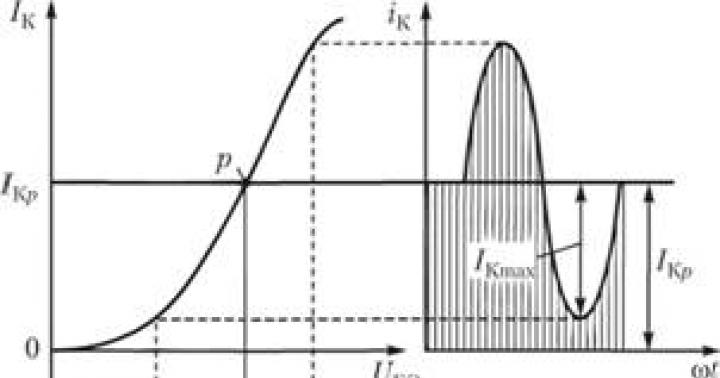
Mode A - is the mode in which the initial operating point R (when the input signal is zero) is located approximately in the middle of the linear section of the characteristic (Fig. 2.10). In this mode, at rest, a relatively large direct current flows through the transistor I Kp, and the amplitude of the variable current component I Kmax is less than or equal to this current. In this case, the shape of the output signal repeats the shape of the input and the non-linear distortions are minimal. According to the efficiency of the cascade, it is only 20–30%, because the useful power is determined only by the variable component of the output current, and the power consumed by the cascade is determined by the sum of the variable I Kmax and constant I Kp components of the output current.

Rice. 2.10. ModeA operation of the amplifying stage

Rice. 2.11.
A - mode IN; b - mode AB
Mode B - this is the mode in which the initial operating point coincides with the origin, i.e. at rest, the output current is zero (Fig. 2.11, A).
When a sinusoidal signal is applied to the input, the current in the output circuit flows only for half a period and has the form of pulses. The efficiency of the cascade in this mode reaches 60–70%, since the constant component I to the collector current (determined by the shaded area as the average value of the current over the period) is significantly less than in the mode A. However, the shape of the amplified signal is too distorted.
AB mode (Fig. 2.11, b) occupies an intermediate position. This mode allows you to reduce non-linear distortion when using push-pull output stages.
Single-ended and double-ended output stages
The output stages are single-cycle and two-cycle. IN single-cycle cascades, there is only one powerful amplifying transistor, which operates both in the positive half-cycle of the sinusoid and in the negative. IN two-stroke cascades - two powerful transistors that work in turn.
Single cycle cascade
The circuit of a single-cycle output stage is similar to the circuit shown in fig. 2.4. The load is turned on instead of the resistor R K, and a decoupling capacitor WITH p2 is missing. Single-cycle cascade operating in the mode A, provides the least non-linear distortion, but has a number of disadvantages: low efficiency; impossibility of application in modes IN And AB due to large non-linear distortions in these modes. Due to these shortcomings, single-cycle cascades are used only at relatively low load powers.
push-pull cascade
It allows you to get rid of the shortcomings inherent in a single-cycle cascade. Such cascades are performed on transistors connected according to circuits with a common emitter or a common collector.

Rice. 2.12.
Usually, in the preliminary stages of amplifiers, the necessary voltage amplification of the input signal is provided, and in the output stage, current and power amplification occurs and a low output impedance is provided. In this case, a push-pull emitter follower is often used as an output stage (Fig. 2.12). The input signal passes through the coupling capacitors and is fed to the bases of transistors VT1 and VT2. These transistors are of different types of conductivity, i.e. VT1 - type r-p-r, a VT2 - type p-r-p. Transistor VT1 is controlled by positive voltage, a VT2 - negative. The positive half cycle of the sine wave of the input signal is amplified by the transistor VT1. At this time, the transistor VT2 is closed and the current flows into the load through the circuit "case - R n – emitter VT1 - collector VT1-- E To ". In the negative half-cycle, the transistors change roles and the transistor works VT2, a VT1 is closed. Current in the load flows through the circuit "+E K - collector VT2 - emitter VT2 - R H – frame".
To ensure the position of the operating point of the transistors, it is necessary to set the bias voltages at the bases of the transistors at rest. For this, chains "resistor RB1 - diode VD1" for transistor VT1 and "resistor R m – diode VD2" for transistor VT2. The current flowing in them provides the necessary bias voltage at the base-emitter junctions of the transistors.
As you can see, the push-pull emitter follower circuit can be divided into two symmetrical parts - the upper and lower, which are called the arms of the cascade. Transistors in this cascade operate in the mode AB. Although each arm gives a large distortion of the sinusoidal signal (in only one half-cycle), together they form the resulting current, which has a sinusoidal shape. Mode AB in a push-pull emitter follower provides low non-linear distortion and high efficiency - about 70%. The disadvantage of push-pull stages is that the parameters of powerful transistors used in different arms must have similar characteristics.
The distortion of the output stage of the amplifier (namely, here they are very significant, compared with the distortion of the preliminary stages) depends on the optimal choice quiescent current(working point) transistors. When moving away from the optimal value of the operating point, the output stage begins to generate high order distortion, which are very negatively perceived by human hearing and are one of the reasons for the "transistor sound" of the amplifier.
Usually, to organize the offset of the output stage, voltage generator. With the relative simplicity of the circuit, it provides an easy setting for the operating point of the output stage. And somehow it just so happened that this knot is not given much importance.
However...
However, for a qualitative amplification of the sound, there are no secondary things, alas.
The output stage bias circuit performs two functions:
1. provides the job optimal quiescent current output stage amplifier (AB mode). Usually, in order to reduce distortion of the "step" type, the output stage is switched to the "AB" mode, despite some loss in amplifier efficiency. In this case, the bias circuit sets the quiescent current of the output transistors on the order of 70-100mA.
2. provides thermal compensation of the quiescent current when the temperature of the output transistors changes. In the "silence" mode, the current through the transistors of the output stage is small - it corresponds to the quiescent current, and the heating of the transistors is not strong. With a large output power, the current through the transistors increases, and their temperature increases significantly.
However, most transistors are characterized positive thermal coefficient, i.e. As the transistor heats up, the current through it increases. As a result, it is possible avalanche self-heating transistor: the current grows - the temperature rises, and if the temperature rises, then the current also rises.
The bias setting circuit should reduce the current of the output transistors when they heat up.
Consider what properties the output stage bias circuit should have.
1. Provide operating point stability with external disturbances: instability of the supply voltage, changes in ambient temperature, etc.
2. Provide the necessary thermal compensation accuracy. For different cascades: emitter followers, Sheklai cascades, etc. requirements for the accuracy of maintaining the bias voltage are different.
3. Provide high temperature compensation speed. When the transistors are heated, the circuit should quickly reduce the current through them, and when cooled, it should also promptly return it to its previous value.
For more than 30 years, a voltage generator with thermal feedback has been used as an element of thermal compensation. Its scheme is quite simple:

To provide thermal feedback, the transistor T1 itself is usually mounted on the radiator of the output transistors.
I note that sometimes there are circuits where the bias voltage is adjusted resistor R1(it is proposed to make it a trimmer). This option is not exactly wrong, but rather dangerous. The mechanical contact of the tuning resistor is very unreliable. It can also be broken due to mechanical reasons or due to oxidation.
In the event of an open circuit in the trimming resistor engine in the presented embodiment, the output transistors of the amplifier will simply close, the amplifier will switch to the “B” mode and this will not bring catastrophic consequences (except for an increase in distortion).
If you make the trimmer resistor R1, then in the event of a break in its engine, the current of the output transistors will increase as much as it can. It is good if the protection circuit (if your amplifier has one) can limit this current in time. Otherwise, you will have to change the output transistors and everything that has time to burn out for one with them.
To ensure the stability of the operating point under various external disturbances, the bias circuit is powered from a current generator:

Here, transistor T6 is a voltage amplifier (pre-output stage), and a stable current source is assembled on transistor T7.
The circuit is quite simple, but it does not take into account "slow" perturbations due to temperature changes: indoors (temperatures can differ significantly in summer and winter), inside the amplifier case. After a long operation, due to the heating of the output transistors inside the device, the temperature increases significantly, and this leads to a change in the current not only of the output transistors, but also of the first stages of the output two / three.
You can compensate for this temperature drift in the following ways:
1. Douglas Self's Diode Method:

2. I. Pugachev's method. In amplifiers of relatively high power, triple cascades are used at the output. At the same time, the output transistors are often installed on radiators, the pre-output transistors - with small heat sinks on the printed circuit board, the first transistors of the trio are usually placed simply on the printed circuit board without a heat sink. The dissipated power of the first transistors is usually small, and here it is only necessary to compensate for the change in voltage Ube with changes in ambient temperature.
To do this, you can use the base-emitter junctions of similar transistors:

For temperature compensation, transistors are combined in pairs (can be glued with back walls) T1 with T4 and T3 with T5. Transistor T2 is attached to the output transistors (more on that below).
The problems of the accuracy of maintaining the set point and the speed of response are best solved together.
The ideal option would be sensors located directly on the crystals of the output transistors. Then both the accuracy of temperature measurement and the speed of response (there are no thermal resistances of radiators, etc.) would be extremely possible.
And today there is such a solution. These are transistor-diode assemblies from the company Thermal Trak:

Here, in one case, a powerful transistor and a diode are placed, which is used as a temperature sensor in the circuit for setting the bias of the output stage.
An example of a power amplifier circuit where such assemblies are used:

Zoom on click.
Unfortunately, these assemblies are quite problematic to find in the vastness of the "great Power", and at the price they "bite" a little. Therefore, a simple radio amateur has to use old-fashioned methods in his amplifiers - use a discrete transistor as a temperature sensor. But even here you need to be smart!
For some reason, it has historically developed that the temperature sensor is most often mounted on a radiator between output transistors:

At the same time, in addition to the thermal resistance "transistor-radiator", a very decent thermal resistance is added radiator section between transistor and temperature sensor. In this case, talk about accuracy And high speed thermal compensation is somehow not logical.
As practice and experiments of Douglas Self show, it heats up the most and cools faster upper surface transistors (side usually marked). Therefore, it will be logical to mount the sensor directly on one of the output transistors:

If the transistors have insulated cases, then a washer between them is optional.
Many probably had a question: which transistor should the sensor be attached to? It is difficult to answer this question unambiguously. It all depends on whether you have an inverting amplifier or a non-inverting one.
It is best to determine the optimal mounting of the sensor experimentally:
1. we fix the sensor according to the "typical" between the transistors.
2. turn on some recording of the choir (Turetsky's choir does not rule in this case)
3. when playing choral records, the transistors of one of the arms will definitely heat up much more than the transistors of the other arm. If it’s a pity to burn your fingers, then even the cheapest Chinese multimeter has a temperature sensor in the kit. You can use it.
4. we fix the transistor-thermal sensor on the most heated transistor.
And in your amplifier, the bias circuit of the output transistors is done correctly ???
© Rod Elliott - 1999-2006
Introduction
I am amazed at the number of amplifier designers who, for one reason or another, failed to address some of the well-known principles and pitfalls of their design during the design phase. While some of these errors (whether from self-importance or ignorance, it is not clear) are of no great importance, others can lead to slow but sure, or even instant destruction of the amplifier's output stages.
My statement "Does not have serious consequences" is perhaps debatable, because. in this context, a sharp increase in distortion is unlikely to destroy anything but the pleasure of the listener.
Even in well-known and respected designs, there can be some fundamental errors - in a lot of "exotic" designs (for example, single-ended open-loop MOSFET stages (ugh with their 5% distortion!), monsters with transformer output, amplifiers are so complicated and bizarre that defy logic or description, etc.), rules are naturally ignored more seriously. This does not cover the tube amplifier section, it is a "special" section and in many applications, such as guitar amplifiers, they remain unrivaled.
In this article, I have tried to cover some of the issues requiring special consideration, and the links at the end are excellent sources for more information on the issues discussed here.
Reference Amplifier
My reference amplifier is shown in Project 3A and I highly recommend it. Since I have repeatedly updated these pages, experimenting both in simulators and in hardware, I eventually found that this amplifier is exemplary. It requires a relatively high quiescent current to keep the output stages away from crosstalk (the "step"), but this can be easily compensated for by using decently sized heatsinks. Even the Class A (Zen Death) circuit does not come close to its average power and is hardly any better at low power.
This amplifier has the following features:
- input stage on a differential pair;
- single-stage voltage amplification stage (A-class driver) with voltage boost;
- output stage on complementary pairs;
- Zobel RC circuit (eliminates the influence of inductances);
- there are no current mirrors or current sources (other than a voltage boost).
It is stable with all common loads, capable of outputting up to 80W into an 8 ohm load, and is easy to assemble. By using only publicly available parts, it is also very inexpensive.
The note: This article is not intended to be a "designer's guide" but is merely a collection of notes and ideas demonstrating the effects of various stages in a typical amplifier. Although I have admitted that some topologies are preferred over others, this does not mean that they should be used automatically. If one were to combine all the "best" configurations into one amp, it does not guarantee that it will perform or sound better than an amp using the "worst" components.
There is a group of developers who believe that the amplifier will be better, the less it uses active components. I don't think this is the case, as my own design philosophy is to make any given project as simple as possible while still meeting the expected parameters.
Other designers will make all sorts of claims about esoteric components, "unexplained" phenomena, or will imply that most known amplifiers are useless for audio because they don't have predictable DC and/or 10 GHz performance, can't be loaded with pure inductance or capacitance etc. and so on. Regardless of these claims, most amplifiers actually work very well and shouldn't do any of the things the applicants might have in mind. The vast majority of all the unusual statements that one might encounter can be safely ignored.
Input stages
There are two basic power amplifier front end circuits. The most common is the differential stage, so we'll cover that first.
Differential Pair
It has been shown that unbalancing the input differential pair properly leads to a significant increase in the distortion introduced by this stage. Some designers try to fix the situation by including a resistor in the "unused" collector circuit, but this is purely a cosmetic solution, since the cascade looks balanced, but this resistor does not play any other useful role (see Fig. 1a). Note that "driver" transistor(sic! So in the original!) serves only to compare the topology of the circuits and ensure the conversion of current to voltage. However, it is worth noting that although this resistor does not play any role in terms of electronics, it can facilitate the layout of the printed circuit board.
The use of a differential amplifier (or "long-tailed" in English terminology - approx. transl.) pairs means that it will work with what is called "voltage feedback" (VOS). Feedback is provided by voltage, as the input impedance of both inputs is high (and approximately the same) and the input current is (relatively) negligible.
The feedback resistor and capacitor are chosen to allow the circuit to operate with maximum AC open-loop gain, but unity DC gain, to keep the stage stable at 0V (or so) across the collector of Q3. The transistors used in the simulations below are "ideal" transistors, with no internal capacitances, etc. and in all cases have a value h FE = 235, measured with a base current of 10 µA. The supply voltage of the simulated circuits is ±12V. Different simulators will give different results, but the trends will be the same.
With a collector current of Q3 = 12 mA, the imbalance of the collector currents of the differential pair will be 94 µA for Q1 and 1 mA for Q2. The situation can be improved by simply reducing the resistance R1, but at the same time the parameters that this stage is capable of will still not be achieved. Again, the gain of the differential stage is quite small, at only 32 (measured at the collector of Q2). The use of R3 is purely cosmetic. It provides a convenient means of measuring the gain of the differential stage, but it plays no other role than that.
Changing the resistance of R1, as a current source, does not affect the gain in any way, but provides a decent improvement in the ripple rejection ratio of the power supply and, in particular, improves the common mode rejection ratio of the signal. A common-mode signal is a signal that arrives with the same phase and amplitude at both inputs at the same time.
The overall gain of this configuration (measured on the collector of Q3) is 842, however, by reducing R2 to 1.8 kΩ, it can be increased to 1850. This also improves the matching of the collector currents of the differential pair, but the specific value will be device dependent and not is a reliable parameter for industrially produced products.

In the scheme shown in fig. 1b, the overall gain is increased to 6860, which significantly improves its performance compared to the previous one. Further improvement in linearity can be achieved by adding resistors (of 100 ohms or so) to the emitters of the current mirror transistors, which will overcome the non-linearity of their base-emitter junctions and provide greater resistance to transistor gain variations. This will not affect the overall gain.
Choosing the right operating current will greatly improve the situation and also help reduce distortion, especially with local negative feedback (as shown in Figure 1b). This has been discussed at length by various authors, and a little bit of simple logic shows that a serious developer deserves an extra boost to their reputation.
Since the value of the internal resistance of the emitter of the transistor (r e) is determined by the flowing emitter current ( I e):

then at very low operating currents it can be quite high. For example, re at a current of 0.5 mA will be about 52 ohms, increasing as the current decreases. Although this resistance will introduce local negative feedback (and reduce the available gain), it is non-linear, leading to distortion due to current variations during normal stage operation. Increasing the current and adding resistors (good and linear ones) to bring the gain back to its previous value will reduce distortion because the resistors, if properly chosen, will "override" changes in the emitter's internal resistance with changes in signal level.
At low currents (when the current changes during operation are relatively large), this internal resistance has a noticeable effect on the performance of the stage. There are many simple solutions to apparently complex problems.
Using a current mirror as a load on the differential pair again improves linearity and gain, providing either deeper local feedback elsewhere, or deeper overall feedback. Any of these options will improve the performance of the amplifier, provided that measures are taken to ensure stability, i.e., the absence of self-excitation at any frequency or any amplitude, regardless of the impedance of the applied load.
Single transistor input stage
There is another (not often used these days) version of the amplifier front end. This is a single emitter feedback transistor. Many have argued that this scheme is significantly inferior to the previous one, however, it has some very pleasant characteristics.

So what's so good about her? In a word: stability. An amplifier using this input stage requires little or no additional stabilization (the "Miller" capacitor, also known as the "dominant pole"), which is mandatory in amplifiers with a differential pair input stage.
An amplifier using this input stage is called a "current feedback" (CTB) circuit because the feedback application point (the emitter of the input transistor) has a very low impedance. The base circuit's input is non-inverting and has a relatively high input impedance, but not as high as a differential pair. Therefore, the +ve and -ve inputs are asymmetric. OCT amplifiers are widely used in extremely fast linear ICs and have a bandwidth of over 300 MHz (that's not a typo!).
This input stage is used in the 10W Class A amplifier (designed by John Linsley-Hood, who is no longer involved with the Audio Pages) as well as the El-Cheapo amplifier described in my project pages. "Okay, if it's so good, why isn't anyone using it?" I heard you ask (then you should have said it quite loudly because Australia is far from here).
There is one major limitation of this circuit that has been "created" by the sudden demand for all power amplifiers to not be shamed by reviewers and rejected by buyers: the ability to accurately reproduce direct current.
(I'm still confused by this requirement because I know for sure that I can't hear the DC signal, my speakers can't reproduce it, I don't know of any musical instrument that could create it, and it would probably be very boring sound, if anyone could apply it.If you don't believe me, put a 1.5V battery in the speaker and let me know if I'm wrong.I seem to remember something about phase shift, which was talked about at the time, but given the acoustics used in studio recording and for playback in a typical listening room, not to mention the "interesting" phase shifts created by loudspeaker cones as a speaker approaches resonance, it seems to me that the effect several degrees of low-frequency phase shift generated in the amplifier is unlikely (assuming, of course, that human ears are able to recognize absolute phase anyway, although it has been clearly shown that they cannot).
This input stage cannot be dc connected (at least not without using a level shifter) due to the voltage drop between the emitter circuit and the base-emitter junction of the transistor. Since such an amplifier cannot be balanced due to the presence of an input stage with an OCT, an isolation capacitance must be present at the input.
In addition, a custom bias circuit design is required and, unfortunately, it must be either tunable (which means a trimmer resistor) or an op-amp must be used to monitor the DC level, which would compare the DC component of the output voltage with a zero reference voltage and would regulate the input voltage to maintain 0 V at the output. The use of such methods will not be discussed here, although they can provide much lower DC bias than can be achieved using the circuitry of the amplifier itself. The op amp has no effect on the sound (considering the discussion that even decent op amps affect the sound anyway) because it only runs on DC (it can have a small effect at a frequency of 0, 5 Hz, but it can hardly be heard).
There is also an opinion that a single transistor has a lower gain than a circuit with a VFO, but this is simply not true. The gain of the open loop feedback stage is at least higher than that of a simple differential pair in the same device.

I modeled a couple of very simple circuits (shown in Figure 2b) to see the difference between them. The collector current for each of them is about 1 mA. The voltage gain at the output of the differential pair circuit is 1770 (it is not possible to correctly measure the voltage gain of the differential input stage alone, since it acts as a current amplifier in both cases). In any case, the DC offset did not interest me, because. it had little effect on simply seeing the gain, so the offset voltage is not displayed. (You will notice that the gains obtained in this simulation are completely different from those obtained earlier for a simple differential pair circuit, because I used a different supply voltage (in the previous example, ± 12V was used). This is by no means nothing cancels, they are just different.
In comparison, the single-transistor open-loop gain is 2000, which is slightly higher, assuming all other parameters remain the same. Admittedly, adding a current mirror will improve the performance of the differential pair even more, but do we really need much more gain? A quick test shows that a gain of 3,570 can be achieved. This looks very impressive, but it is only a little more than 4.2dB of gain compared to the single transistor circuit. By the same logic, a single transistor circuit has a mere 1.06 dB advantage over a simple differential pair, however, this difference can be moot...
Since a single transistor stage does not require a Miller capacitor (dominant pole) to ensure stability, it will maintain gain over a much wider bandwidth, so it can be much better than a differential pair in the long run. Obviously, further tests were required, which I performed. Real life is never quite like the simulated version, so the gain of each circuit was slightly less than what the simulator showed. The gain of the open-loop differential stage was found to be 1000, while that of the single-transistor stage was 1400. The test conditions differed slightly from the simulation in that a ±15V supply voltage was used, so the difference in gain was about the same as expected and very close to the ±12V power results obtained in the first set of differential pair simulations.
The nature of the distortions was interesting. For the differential pair, they were 0.7%, formed mainly by the 3rd harmonic. At the same output voltage, the single-transistor stage turned out to be slightly worse with its 0.9% and the predominance of the 2nd harmonic.
As expected, without the Miller capacitor, the differential pair was unstable, it was managed to tame it with a 56 pF capacitor. Quite unexpectedly, the single transistor also required a Miller capacitor, but only in open-loop operation. When the feedback loop was restored, the self-excitation disappeared. The differential stage could not be used without a Miller capacitor at any gain, and as the gain approached unity, a larger capacitance was required to prevent self-excitation.
The next step was to test each circuit with a gain around 27 as it approaches the "normal" value for a 60W power amplifier. Here, the differential pair has a clear advantage in terms of distortion, which I could not measure. The single transistor circuit had 0.04% distortion and again, it was predominantly 2nd harmonic. In this mode, the single-transistor stage does not require a Miller capacitor and exhibits very wide bandwidth with little increase in gain above 100 kHz. This was also noticeable with the 10 kHz square wave having overshoot, although it was quite similar to the positive and negative half cycles. The differential stage behaved well and showed no overshoot (a 56 pF Miller capacitor was installed in it), but the gain began to decrease at about 80 kHz, and there were signs of slew-limiting. In a single-transistor cascade, this effect did not appear.
It seems to me that overall it was a useful experiment and the use of a simple resistor as the collector load of the voltage amplifier stage allowed the complete circuit to have a controllable gain. If a current source or something similar was used as a load, I would not be able to accurately measure the gain, because. the input levels would be too low. Be that as it may, noise reduction turned out to be a serious problem, and without the possibility of averaging the signal on an oscilloscope, it was difficult to obtain accurate results.
conclusions
Based on the tests, there are pros and cons to both input stage designs and I bet it came as a surprise. The differential stage in its simple form is a clear loser for amplification, however, the use of a current mirror allows it to bypass the single transistor stage, for which this technique is not suitable, because. there is nothing in it that can be "reflected".
Stability is very important to me and I lean towards an amplifier that is absolutely not prone to self-excitation, even at the expense of a little more distortion. My own basic 60W amplifier using a differential pair in the front end is unquestionably stable with normal loads.
RFI protection
A favorite technique of many developers is to connect a small capacitor, as shown in fig. 3, directly to the base of the input transistor. This is supposed to prevent the detection (rectification) of RF signals picked up by the input wires. To a certain extent, this is true, because. the resistor-capacitor (RC) combination forms a low-pass filter that reduces the amount of RF noise applied to the input. With the ratings shown in the figure, the 3dB bandwidth is 159 kHz.

Things get extremely frustrating if the level of RF interference is so high that it somehow manages to crawl through everything anyway. I used to have a workshop/laboratory with three broadcast television towers around it - very disgusting.
The traditional method not only didn't work, but even worsened the situation, due to the fact that the bases of the transistors were powered from a source with a very low impedance due to the presence of the capacitor C1 (in terms of radio frequencies). A huge number of commercial amplifiers and other equipment that I was working on at the time received completely unacceptable levels of noise in the television range due to the detection of V-sync pulses of the 50 Hz television signal. Since the TV picture component is an amplitude modulated radio frequency, it was easily converted into the most unpleasant kind of sound.

On fig. Figure 4 shows the remedy, but to be effective, R2 must be placed as close to the base of the transistor as possible, otherwise the performance is degraded. How it works? It's just that the emitter-base junction of the transistor is a diode, and even with its direct conduction, nonlinearities will remain. They are often sufficient to make the front end work as a coarse amplitude detector, effective enough with high frequency television or medium wave signals. Adding an external resistance again reduces the internal non-linearities, reducing the diode effect to a negligible amount. This does not mean that it will completely eliminate the problem in the presence of a strong RF field, but will reduce it to at least an "uncomfortable" level, not an "unbearable" one.
UPDATES E: A reader working at a transmitting station has suggested that it is very efficient to connect a capacitor directly between the base and emitter (in combination with a notch resistor). He also found that the traditional method was useless and that in the presence of strong fields, a simple stopper was not enough.
With op-amps, the equivalent solution is to put a notch resistor in series with the non-inverting input and put a capacitor between the inverting and non-inverting inputs without a connection to ground.
In all cases, it is important that all PCB leads and traces are kept to a minimum length so that they cannot act as RF antennas. Needless to say, a shielded (and grounded) equipment enclosure is a must in such environments.
Voltage Gain Stage (Class A Amplifier)
The voltage amplification stage (VCH) is also widely known as the A-class driver. Both of these terms are generally accepted and are usually used interchangeably. There are several pitfalls here, not least due to the fact that it is common to assume that the load (of the output stage) is infinite. Oh, of course, every designer knows that the voltage boost stage must exceed the current that the output stage must draw by at least 50%, and it is easily calculated:
 ,
,
Where: I A- A-class stage current (voltage amplifier);
Peak_V- maximum (peak) voltage at the load;
Op_R- load resistance;
Op_Gain is the gain of the output stage transistors.
For a typical 100W amplifier loaded into 8 ohms, this will be somewhere between 5 and 10mA. Assume that the input impedance of an output stage with a gain of 1000 (50 for the driver transistor and 20 for the power transistor) loaded into 8 ohms would be about 2 kΩ for the voltage gain stage, which is still slightly different from infinity.
Added to this is the fact that the impedance reflected back is non-linear, since the current gain in both the driver and output transistors, as in all real semiconductors, is not stable. Now there are some types of transistors that are much better than average, but in this respect they are still not perfect.
For a stacked pair of transistors, the voltage gain is typically between 0.95 and 0.97. It should be noted that this indicator is valid only for average values of collector currents and will decrease at their lower and higher values. On fig. Figure 5 shows a common configuration for this stage - the same basic amplifier we used earlier, with the addition of a current source as a collector load. Also common is the bootstrap circuit, not shown here but evident in many ESP circuits.
There is not much difference between current source and voltage boost circuits, however, the current source circuit has a slightly higher gain. For any of the circuit designs, there are some very simple additions that improve linearity quite substantially. On fig. Figure 5 shows a typical arrangement, including a 100 pF Miller correction capacitor connected between the collector and base of the voltage amplification transistor.

Therefore, it is important to try to make the voltage amplification stage capable of high gain, even when the output stage is heavily loaded. Many different methods have been proposed to achieve this, but none have been completely successful. The biggest problem is that many developers seem to be completely oblivious to this critical moment, or create such amazingly complex "solutions" that are almost impossible to maintain stability.

The solution shown above in Fig. 6, simple and very effective. Simply adding an emitter follower to the voltage boost stage (with a 1k ohm boost resistor) increased the overall gain of the differential stage, together with the voltage boost stage, to 1,800,000 (yes, 1.8 million!) or 125 dB (with an open loop back). connection and without a Miller correcting capacitor). The open-loop output impedance is about 10 kΩ, again without the correction capacitor. With it (with a value of 100 pF shown in the diagram), the gain decreases to a slightly more reasonable 37,000 at a frequency of 1 kHz. The output impedance at 1 kHz in this case is comparatively very low - about 150 ohms.
Note that in the example above, a 5 kΩ resistor is used instead of a conventional current source. This is only for the simplicity of the circuit, and not to suggest that the current source should be like that.
A special note to the unwary: if you wish to use transistorized current sources for both the differential stage and the voltage amplification stage (aka "VAS"), do not use the reference voltage of the voltage amplifier's current source (aka A-class driver) as the source reference. differential stage current. If this is done, then the changing current in the voltage amplifier circuit will cause the current of the emitters of the differential stage to be modulated. The results are bound to be as undesirable as they are unpredictable.
I have often seen amplifier designs so complex that I wondered how they ever managed to prevent high frequency self-excitation. The sometimes used labyrinth of small capacitors (some with a series resistor, some without) really makes one wonder what an open-loop bandwidth and phase response should look like. Pair this with the fact that many of these amps don't have superior performance at all, and consider what the designer was actually trying to create (in my opinion, the "distinctiveness" of these circuits is not a valid reason for publishing or promoting them, unless they do not imply any bonuses that are unattainable in other ways).
UPDATE A: After doing quite a few experiments over the course of several weeks, I'm still not completely convinced that a huge input stage gain is necessary or even desirable in combination with a voltage amplification stage. The end result is most likely to be satisfactory as long as the circuit is linear (i.e., has a low level of distortion before the feedback loop is closed). I have seen many circuits with much higher loop gain than my basic amplifier (Project #3A) that should theoretically be significantly better, but they are not.
Active current source or voltage boost (bootstrap)?
An easier way is to use a voltage boost circuit, which uses a capacitor connected to the output to maintain a relatively constant voltage across the resistor. Since the voltage across the resistor is stable, it follows that the current flowing through it must also be stable. On fig. 6a shows a diagram of a stable current source with a voltage boost. Unlike a true current source, the current through the boost circuit will change with the supply voltage. This change is gradual and lies outside the band of the reproduced sound, or so (if the circuit is designed correctly) at least it should be.

This scheme works as follows. At rest, the output voltage is zero, and the positive supply voltage is divided between R b1 and R b2 . There will be about +0.7 V at the base of the top transistor - enough to bias it. Since positive or negative deviations of the output voltage are transmitted through C b , the voltage across R b2 remains stable. Therefore, the current through R b2 is stable, because it is maintained, in fact, by maintaining a stable voltage on it. Please note that this only applies to AC voltage, as the capacitor will only recharge if there is a change in DC voltage.
In the full design, the differences are small. Although the current source is theoretically better, the voltage boost circuit is simpler and cheaper and does not require the introduction of any additional active components. The capacitor must be large enough to ensure that the AC voltage drop across it remains small (less than a few hundred millivolts) at the lowest frequency of interest. Assuming that the resistances R b1 and R b2 are equal, the rated operating voltage of the capacitor should be at least ½ of the positive supply voltage, but preferably more.
Output stage
There are countless amplifiers that still use the composite Darlington pair in the output stage, despite being shown by many to be inferior to the complementary Shiklai pair. Both schemes (in their basic form, since there are many variants of them) are shown in Fig. 7. There are two main areas where the Darlington circuit is worse and we will look at both.

From the two configurations shown, it's obvious that I didn't include field effect transistor (FET) output stages in this list because FETs don't need any driver transistor per se - they're usually driven directly from the voltage boost stage (or a modified version - often modified by a differential stage). For those shown in Fig. 7 modifications, the number of components is the same, but instead of two transistors of the same polarity (two PNP or two NPN), a complementary pair (also called a Shiklai pair) uses one transistor of each polarity. The completed compound circuit has the characteristics of a driver transistor in terms of polarity, so the emitter, base, and collector pins are shown for each configuration. The resistor is added to prevent the output transistor from opening on its own due to the presence of leakage current between the collector and the base, as well as to accelerate the closing. The absence of this resistor is not a common mistake, but it is still often done. The result is increased distortion, especially at high frequencies, and poor thermal stability.
The value of this resistor must be chosen with sufficient care. If it is too small - the output transistor will not be ajar at rest (no signal), the driver transistor(s) will dissipate excessive heat, resulting in "step" distortion. If the resistance is too high, the turn-off efficiency of the output transistors will be compromised and thermal stability will deteriorate. The final value depends (to some extent) on the current of the voltage amplification stage and the gain of the driver transistor, but the final indicator of the magnitude of the quiescent current is the total value of V be of the output stage transistors. These comments apply equally to both Darlington and Shiklai couples.
For most amplifiers, values from 100 ohms up to a maximum, possibly up to 1k ohms, are acceptable, with lower values applied as the power increases. High power requires higher currents to flow through the output stage and, again, impairs transistor turn-off, especially at high frequencies. This can lead to a phenomenon called "cross conduction" ("through currents"), which occurs because the transistors cannot turn off quickly, so there is a period when both power transistors conduct at the same time. This will not happen when playing the normal audio frequency range, although the power supply may require a slightly higher current draw than usual, even at 20 kHz.
If the amplifier is operated at any reasonable power at higher frequencies, with sufficient cross-conduction present, it may spontaneously fail. The easiest way to reduce this risk is to use smaller resistors between the base and emitter of the power transistors, but keep in mind that this will increase the requirements for driver transistors. For example, with 220 ohm resistors as shown above, only 3-5mA of current will flow through them, but if they are reduced to (say) 47 ohm, then the current through them will increase to 16mA or even more. Drivers must provide this current even at idle, and their power dissipation rises from 120mW to over 550mW at ±35V supply voltage. A heatsink becomes necessary for the driver transistors.
As a rule, only in rare cases or at all it is not necessary to use resistors less than about 100 ohms. If you want to get full power at 100kHz or more (and why? It's not meant for an audio amplifier), then these resistors need to be even lower when combined with the appropriate heatsinks for the driver transistors. You will also need to increase the rated power of the Zobel circuit resistor, otherwise it will overheat at high frequencies.
thermal stability
Obviously, in the Darlington configuration, there are two base-emitter junctions in each output stage. Since each has its own thermal response (reduction in voltage drop across the junction by about 2 mV per degree C), it can be difficult to thermally stabilize this configuration. Also, as transistors get hotter, their gain often increases, further complicating the problem. The sensor of the quiescent current setting circuit, which, as a rule, is a V be transistor multiplier, must be installed on the radiator of the output transistors in order to ensure good thermal contact with them, and in some cases thermal stability can hardly be maintained.
If sufficient thermal stability is not ensured, then an avalanche-like increase in the temperature of the output stage transistors can develop in the amplifier, where, after reaching a certain temperature of the output transistor, the continued decrease in V be causes an even greater increase in the quiescent current, which leads to a further increase in temperature, etc. A point is reached where the power dissipation is so great that the output transistors fail, often with catastrophic consequences for the rest of the circuit and/or connected loudspeakers.
The complementary Shiklai pair has only one controlled base-emitter junction and, thus, it is easier to thermally stabilize it. Since the only V be is that of the driver transistor (which in many cases will not be mounted on the main heat sink, and some will not have a heat sink at all), the requirements for the V be multiplier are less stringent, mounting is much easier, and thermal stability is generally very good and excellent.
I have been using the complementary pair since the early 1970s, and when I first saw it, I had plenty of reason to ignore it. Thermal stability in a fairly simple 100W 4 ohm amplifier of my design (the forerunner of Project #3A, of which many hundreds have been assembled) was provided by a simple two-diode circuit that required no tuning (however, there were a few other tricks at the time to ensure stable operation. ).
Bias circuit design
It would seem (at least at first glance) that there is nothing complicated in this knot. It is a very simple V be multiplier circuit and it seems that, contrary to what was intended, nothing can happen in it. This is almost true, except for the following points.

Many amplifier designs (especially those using a Darlington output stage) require that the bias circuit be tuned to accommodate various output transistor settings. If the resistor R1 (in Fig. 9) instead of a constant one is a trimmer, then what happens when (if) its moving contact suddenly (due to age, dirt or rough handling) loses contact with the resistive track?
The answer is simple - the voltage drop across the bias circuit will now be equal to the full supply voltage (less than the drop across one or two base-emitter junctions), as a result of which both positive and negative arms of the output stage will open as fully as possible. The result of this is instantaneous failure of the output transistors. This will happen so quickly that the fuses cannot prevent it, and even the use of a complex output circuit protection scheme is unlikely to save them.
The answer, of course, is so simple that it should be immediately obvious to everyone, but, unfortunately, this is not always the case. If R2 is made a variable component, then when it breaks, the shift will simply disappear. This will lead to the appearance of distortion in the form of a "step", but the output transistors will remain intact. To prevent the possibility of reducing the value of the trimmer resistance to 0 ohms (which will have the same effect as described above!), a constant resistor should be connected in series with it, the value of which should be chosen in such a way as to provide adequate tuning while maintaining a reliable margin of safety.
Extra care must be taken here, because if the base divider resistor values are too low, then the bias voltage created for the output transistors will simply be a voltage drop across them. In this case, the bias circuit transistor will have practically no effect on the bias value. This can easily be avoided by making the current through the base divider resistors equal to 1/10th (or so) of the total bias current of the voltage amplification stage.
The resistance can also be made too high, making the bias circuit less ac stable. Because of this, the bias circuit can also gain too much gain, which in turn can cause the quiescent current to drop as the amplifier heats up. While this is good from a reliability point of view, since the amp will generate “step” distortion as the amplifier heats up, the sound effect will obviously be disappointing. As a general rule, experiment with the resistor values of the base divider to ensure stability. There is no way to calculate them, although I am sure that this is possible. The voltage drop across the base-emitter junction is reduced by up to 2 mV/°C, however, the change in gain with temperature is not as easily calculated.
As a secondary protection, it is useful to put a chain of the appropriate number of diodes in parallel with the bias circuit. They should be chosen to prevent overcurrent, however, in addition to them, some other method of protection against overheating is needed. This could be a fan blowing over a heatsink, or a thermal switch to turn off the power if the amp gets too hot.
Note that if the output stage uses a Darlington circuit, the bias transistor will be located on the main heatsink. If a complementary pair of transistors (shiklai) is used, it is necessary that the bias circuit sense the temperature of the driver transistor(s) (which should not be on the main heatsink. Misplacement of the bias circuit transistor is an invitation to output stage failure due to thermal runaway.
Linearity
Numerous articles have been written about the superior linearity of the complementary (Shiklai) configuration (Otala, Douglas Self, Linsley Hood, etc.) and I can't help but be surprised when I see a new circuit in a magazine still using the Darlington configuration. The use of a complementary pair does not require more components - the same components, just connected differently. With great pleasure, an Australian electronics magazine proudly announced (in 1998) that "we used this circuit for the first time in a published design" (or something like that). I don't know why they might not have used the complementary pair in every project they published (this journal is much younger than me). I have no words. The magazine in question is not the only one, and the Internet is replete with old and new designs using Darlington emitter-followers.
This is not to say that the Darlington circuit should not be used - there are many good amplifiers that use it and with some extra effort to achieve the correct bias, such amplifiers will provide many years of reliable performance. The Darlington circuit is particularly suitable for high power amplifiers due to its simplicity, especially with multiple output transistors in parallel. Parallel inclusion of the Shiklai configuration is more difficult. An example of Shiklai's parallel pairs is shown in Project #27.
Relative Current Gain of Shiklai Complementary Pair Compared to Darlington Emitter Follower
The lower gain of the complementary pair of transistors indicates the presence of internal local negative feedback inherent in this configuration, and all tests performed show that this is indeed the case. Although the gain difference is small, it can be assumed that most of the increased linearity is due to the fact that only one base-emitter junction is directly involved in the signal path, and not two, as in the Darlington circuit, so only one set of direct non-linearities is introduced into the equation . The second (output) transistor effectively acts as a buffer for the first (driver).
It should be noted that there are several very well-established amplifiers with compound Darlington pair output stages. There are no hard and fast rules that can be applied to building the perfect amplifier (especially since it doesn't exist yet), and with proper design it is quite possible to build a very good audio amplifier using almost any topology.
Output Stage Stability
That an emitter follower (be it a Darlington or Shiklai) can become an oscillator, usually at very high frequencies, is simply a fact of life. This is especially true if the output cable is in the form of a tuned circuit. The length of the cable to the speakers, while perfectly harmless at audio frequencies, is a transmission line at some frequency, determined by its length, the diameter of the conductor, and the distance between the conductors. The ARRL Handbook (any year of publication) will provide all the formulas you need to calculate if you really want to delve into this issue.
All power amplifiers (well, almost all) have emitter-follower output stages, and when a speaker (or even a non-inductive equivalent load) is connected to them by cable, self-excitation often occurs. This happens almost always when the amplifier is running, and is more likely if current is being drawn. It is a little sad that the Shiklai complementary pair is more susceptible to this sad phenomenon compared to the Darlington pair, perhaps because the control element is a driver transistor (its emitter is connected to the load), which has a wider bandwidth.
Some of the "super" cables (much loved by audiophiles) are often worse in this respect than a regular shielded cord or a three-wire mains cord, due to their ability to act as RF transmission lines - fig. 8 ( missing from the original article! - approx. per.) and are therefore the source of said problem.

A conventional Zobel circuit (consisting of a 10 ohm resistor and a 100 nF capacitor) will generally dampen the influence of the external cable transfer line and amplifier internal wiring to the output terminals and provide stability under most normal operating conditions.
At these frequencies, the Zobel circuit capacitor is essentially a short-circuited jumper, so a 10 ohm resistor is included in parallel with the high impedance circuit. A 10 ohm resistor breaks the quality factor (Q) of the tuned circuit(s) and provides a lot of damping, thereby canceling the phase shift and restoring stability. Personally, I do not recommend removing this circuit from any amplifier, even if it seems stable without it.
With a capacitive load (as happens when connecting a loudspeaker and a passive crossover), the Zobel circuit has very little additional effect and may not have any effect at all. The only sure way to prevent self-excitation, or a pronounced ringing when using cables with high capacitance, is to turn on the output of the amplifier inductance. It must be shunted with an appropriate resistor to reduce the quality factor of the inductance. A typical circuit is shown in Fig. 10. For readers wishing to explore this in more detail, read The Audio Power Interface. In many cases it would be better to use a much lower resistance than the commonly used 10 ohms - about 1 ohm or so, I think. In some National Semiconductor power amplifiers, the optimum value is 2.7 ohms. Ideally, low inductance, high capacitance cables should always have an additional 100nF/10Ω Zobel circuit at the speaker end. When this is done, the cable at high frequencies will no longer be perceived as a capacitor. Unfortunately, few speaker manufacturers (if any) find it worthwhile to put this circuit on the speaker input terminals.
Another alternative is to put a resistor in series with the amplifier output, but this will naturally have the double effect of reducing output power and damping factor. With resistor values sufficient to prevent self-excitation, the above losses become excessive and all the lost power must be converted to heat in the resistor.
The choice of inductance value is not difficult - at a load of 8 ohms it should, as a rule, be no more than 20 μH, and any inductance greater than specified will lead to unacceptable attenuation of high frequencies. Choke inductance 6uH, as shown in fig. 10 will result in a loss (assuming its resistance is 0.03 ohms) of 0.03 dB at low frequencies and about 0.2 dB at 20 kHz. These losses are insignificant and will not be heard. In contrast, ringing (or, in extreme cases, self-excitation) of the output stages will be audible (even at very low levels) as an increase in distortion, and in extreme cases can even destroy the output transistors.
Self-excited transistors
This is not obvious to everyone, but a transistor cascade can be self-excited even with unity gain. Op-amps and power amplifiers usually use emitter followers at the outputs, and failure to isolate the transistor stage from the influence of the connecting cable can cause the stage (and regularly does) to self-excite. All op amps connected to external peripherals (for example, via front or rear panel connectors) must use a series resistor. As a rule, values from 47 to 220 ohms are sufficient. I usually use 100 ohms, but lower (or higher) values may be needed, depending on what you want to achieve.

In simulators and on a lab bench, I was able to construct a single-transistor emitter follower circuit (shown in Figure 11) gleefully self-excited with an actual transmission line load (such as a length of coax cable) or composed of its equivalent 500 µH inductance and 100 µH capacitance. pF as a tuned series circuit.

This effect worsens as the source impedance decreases, but even a basic plug resistor does not prevent self-excitation. It will only be effective to silence the transmission line with a Zobel circuit or series resistance. In case you are wondering why the oscilloscope is connected to the junction point of inductance and capacitance - this allows the series resonance to amplify the high frequency component, making it more visible.
For power amplifiers, this problem is solved with a Zobel circuit, optionally with a series inductor. For small signal stages, it makes more sense to use a resistor in series with the output. Usually the resistor value is between 22 and 100 ohms and this will be seen in all ESP designs where the op-amp is connected to an external load (or even to an internal cable). The resistor can also be used with power amplifiers, but at the cost of power loss, increased heat dissipation, and loss of damping factor. For a power amplifier, the output inductance can be replaced by a 1 ohm resistor (sometimes less), but this is very rarely done.
In my own amplifier (latest incarnation - Project #3A) I did not use the output inductance, but instead put a correction capacitor (between the collector and the base of the voltage amplification stage transistor) with a capacitance slightly larger than usual. This made it possible to stabilize the amplifier in all operating modes, but at the expense of the slew rate (and, as a result, the limited power slew rate at high frequencies). This was largely an economic decision, since a pair of ceramic capacitors is much cheaper than an inductor, and the amplifier was used at the time mainly to amplify musical instruments, so an upwardly extended bandwidth was effectively undesirable. Full bandwidth - the ability of an amplifier to deliver full power over the entire operating frequency range - is a sure way to damage hearing, tweeters (etc.) in live music environments, so this trade-off was not limiting. However…
There is another reason why a series output inductor can be useful. It has been suggested (but I don't remember by whom) that radio frequencies received by the wires leading to the loudspeakers can be fed back to the front stage through negative feedback. If you look at a typical circuit, this seems plausible, but I have not tested this theory too deeply.
However, it is not so difficult to take into account the basics of this when developing. Since it is known that in the frequency response of an amplifier with an open feedback loop there should be a dominant pole (the capacitor shown in Fig. 5 and 6), then from the fact that if it remains stable when the feedback loop is closed, it follows that as internal gain with increasing frequency, the output impedance must increase (because of the shallower overall feedback). This is true, and by the time the frequency gets into the megahertz region, the output stage will have a negligible load for any such frequencies.
If appropriate precautions are not taken (as shown in Figure 4) for the negative feedback loop, it is likely that RF interference detection may occur. In my own two-channel system (which uses the precursor to the Project #3A amplifier described above, still without output inductance), I myself have recently had trouble finding a local AM radio station. Installing RF suppression chokes (basically a loop of cable to the speakers 3 or 4 times through a ferrite ring) completely eliminated this problem, so I must conclude that this is indeed likely or even possible.
If "exotic" (expensive "audiophile") cables are ever to be connected to the amplifier, it is important to use the output inductance. As noted above, the inductance must be limited to prevent high frequency roll-off, and for load resistances up to 4 Ω, the inductance must not exceed 10 µH. In most cases, the number of turns placed across the 10 ohm 1W resistor will suffice, and the wire used must be thick enough to carry the full current to the speaker.
Output current
The maximum output current of a power amplifier is often considered to be something only the output transistors affect, and to lower the impedance, adding more transistors will automatically provide more current. This is partly true, because bipolar transistors need a base current, which must come from the driver stage.
Typically, biasing the voltage amplification stage allows for 1.5 to 5 times the base current required by the output transistors and their drivers. If the output current of this stage is not sufficient, then distortion is likely to increase significantly as the current changes by a larger amount. If the current of the voltage amplification stage is too high, then the transistor will generate too much heat, which will have to be disposed of, and in this case, the maximum allowable parameters for the transistor can be exceeded. I usually work with a figure on the order of twice the expected output stage current, but in some cases it will be more or less. The design should also consider the lowest expected current gain of all transistors used.
As an example, consider a typical power amplifier output stage. Assuming a power supply voltage of ±35V, the maximum (peak) output current would be 35/8 = 4.375A (assuming a load of 8 ohms). Since we know that there will be some losses in the driver/power transistor combination, we can safely assume that the maximum (peak) current is 4 A. A suitable power transistor can be specified with a minimum gain (h FE) of 25 and a collector current of 4 A. Driver transistors typically have a higher gain, perhaps 50 at a collector current of 250 mA. The product of the two current gains is accurate enough for what we need and gives the final h FE = 1000. So the maximum base current would be 4 mA.
If we decide to use a voltage boost stage current equal to twice the expected output stage current, then this means that the driver will operate with a current of approximately 8 mA. This current value can be achieved using either a current source or a voltage boost circuit using a pair of 2.2 kΩ resistors in series. At the maximum output voltage swing (close to ±35V), the driver current will increase to 12mA or decrease to 4mA, depending on the polarity. The current source or voltage boost will keep the current stable, but the voltage amplifier has to deal with a current that changes by ±4 mA as the load current changes.
If the load impedance drops to 4 ohms, then the current source will still only be able to supply 8mA, so the output current will be limited to 8A because the driver has zero current at that point in the cycle. At the opposite extreme, the driver will have to handle 16mA when it is fully open. At even lower resistances, the driver will be able to deliver more current, but the current source will steadily refuse to deliver more than the 8mA it was designed for, so the maximum output current will be limited to 8A in one direction (when the stage output is provided by the current source). , and the transistor of the voltage amplification stage is closed) or some other (possibly excessive) maximum current in the opposite polarity.
However, attention!! The voltage amplification stage (A-class driver) is called so because it should never be turned off - now we have an AB-class stage, which is not only undesirable, but even unusable for a single-ended output stage! The output of the power amplifier will be clipped asymmetrically and is no longer in the linear range - it is distorted.
Adding more powerful transistors will only provide very limited benefits. the maximum base current is still limited by the current source feeding the voltage amplification stage. To get maximum power at lower load resistances, either increase the gain of the output stage or increase the output current of the voltage amplification stage. Increasing the gain of the output stage transistors is not trivial - either a different topology or driver and output transistors with a higher gain should be used.
The amplifier design phase is driven by similar principles, regardless of topology. "The Principles of Operation of an Amplifier" ...
Output power versus load resistance
The output power is determined by the load impedance and the available output voltage and current of the amplifier. An amplifier capable of delivering a maximum output current of 2A will not be able to deliver more just because you want it. Such an amplifier will be limited to an output power of 16 watts "RMS" into 8 ohms, regardless of the supply voltage. Likewise, an amplifier with a ±16V supply will not be able to deliver more than 16W RMS into 8 ohms, regardless of its current output capability. With the ability to deliver more current, the amplifier will be able to deliver (for example) 32 watts into 4 ohms (4 amps peak) or 64 watts into 2 ohms (8 amps peak), but will not deliver more power into 8 ohms than the supply voltage will allow. .
Driver stage current
The driver stage, especially when using bipolar transistors, must provide sufficient current for the output transistors. With MOSFETs, the driver must be able to charge and discharge the gate-source capacitance fast enough so that the required power can be obtained at the highest frequencies of interest.
For simplicity, if the bipolar output transistors have a gain of 20 at maximum load current, the drivers should be able to provide enough base current for this. If the maximum current is 4A, then the drivers must be able to provide the output transistors with 200mA of base current.
Voltage amplification stage
The stages before the driver transistors must be able to provide enough current for their load. The voltage gain stage of a bipolar or MOSFET amplifier must provide enough current to meet the base current requirements of the bipolar drivers or the gate capacitance of the MOSFETs.
Again, using the example given earlier with bipolar transistors, the maximum base current for the output transistors was 200 mA. If the drivers have a minimum gain of 50 then their base current will be:

Since the voltage boost stage needs to operate in mode A (what a surprise, right?!), it will need to operate with a current of 1.5-5 times the expected maximum base current of the driver transistor so that it never turns off. The same applies to the MOSFET amplifier, which will expect (for example) the maximum current to charge (or discharge) the gate capacitance at 4 mA at the highest amplitudes and frequencies. For the purposes of this exercise, we will assume that the voltage amplification stage (VAS) current is equal to twice the base current requirements of the driver transistors, i.e. 8 mA.
Input stages
The input stages of all transistor amplifiers must supply base current to the voltage amplification stage. This time, the required current is 2 to 5 times the expected maximum base current of the voltage boost stage. If the voltage boost stage operates with a quiescent current of 8 mA, then its maximum collector current will be 12 mA (DC + driver base current). Assuming a gain of 50 (again), this means that the front end must be able to deliver 12/50 = 240 uA, so it must operate at a minimum current of 240 uA x 2 = 480 uA to maintain linearity.
Input current
The input current of the first stage determines the input impedance of the amplifier. Using the collector current figure above of 480µA, the base current of the input transistors having a gain of 100 would be 4.8µA. If the amplifier is designed to operate with an input voltage of 1 V at maximum power, then the impedance is: 208 kΩ (R = V/I).
Since this stage must be biased, we apply the same rules as before - the range limits are from 2 to 5, so the maximum value of the bias resistors should be 208/2 = 104 kΩ. A lower value is preferred and I believe a factor of 5 is more appropriate, giving 208/5 = 42 kΩ (47 kΩ can be used without problems).
These are only recommendations (of course) and there are many cases where the current is more (or less) than expected. The end result is the sound of an amplifier and the approach described in the tutorials does not always give the expected result.
Some notes on power supply design
As you know, the behavior of the transformer is described with a resistive load for a full cycle, but if there is a capacitor filter after the rectifier (99.9% of all amplifier power supplies), the calculated and measured figures will never match.
Since for a fairly long period of time the AC voltage from the secondary winding of the transformer is lower than on the capacitor, then during this time the rectifier diodes do not conduct current. During the short periods when the diodes turn on conductive, the transformer must make up for all the energy drawn from the capacitor between the open states of the diodes, as well as provide an instantaneous output current.
Consider the power supply shown in fig. 13. This is a completely conventional full-wave rectifier with a capacitor filter (for convenience, it is shown as unipolar). It is assumed that the circuit has a total effective series resistance of 1 Ω, formed by the resistance of the transformer windings (primary and secondary). Capacitor C1 has a value of 4,700 uF. The secondary voltage of the transformer is 28 V. About 760 mV will drop across the diodes at full power.

The transformer is designed for 60 VA and has a primary winding resistance of 4.3 ohms, a secondary winding of 0.5 ohms. These impedances are converted to an internal copper loss resistance of 1.0 Ω.
With a load resistance of 20 ohms, as shown in the figure, and with an output current of 1.57 A, the conduction time of the diodes is about 3.5 ms, and the peak value of the current flowing into the capacitor 100 times per second is 4.8 A (with an interval at 10 ms). Therefore, the conduction time of the diodes is 35% of the cycle time. The rms current in the secondary winding of the transformer is 2.84 A.

The voltage ripple across the load (peak-to-peak) is 2.2V (692mV RMS) and is expected to be sawtooth. The average DC voltage will be 31.6 V. The no-load supply voltage will be 38.3 V, so with an output current of 1.57 A, the losses will be:

Where V n- voltage without load;
Vl- voltage under load.
For this example, this is close enough to 17%, which is hardly a good result. For comparison, the actual loss in the transformer would be 8% for an output current of 2.14A at 28V. Note that the rms AC current in the secondary of the transformer is 2.84A ) for a DC output of 1.57 A - this should be so, because otherwise we would get something for free - contrary to science and the tax collector.
The output power is 31.6 V 1.57 A = 49.6 W, and the input power is 28 V 2.84 A = 79 VA.
The input power of the transformer is 60W, so the power factor is:
There are many losses to consider, most of which are due to the voltage drop across the diodes (600mW per diode, 2.4W in total) and across the transformer winding resistance (8W at full load). Even the equivalent series resistance (ESR) of the capacitors adds a small amount of loss, as does the mains wiring. There is also an additional loss in the "iron" of the transformer core - this is the sum of the current required to maintain the level of magnetic flux in the transformer, plus eddy current losses that heat the core. Iron losses are most significant at no load and can usually be ignored at full load.
Although the transformer is overloaded for this example, as long as the overload is momentary, there will be no damage. Transformers are usually rated for average power (VA) and can withstand large overloads, provided that the average value is not exceeded in the long term. The duration of the permissible overload is largely determined by the thermal mass of the transformer itself.
![]() Capacitor ripple current. It is well known that larger transformers perform better than smaller ones, so it is common practice to use a higher power transformer for this application. This can greatly improve efficiency, but will also create higher voltages across the filter capacitor due to the higher ripple current. This parameter is indicated in the manufacturer's datasheet for capacitors intended for use in power supplies and must not be exceeded. Excessive ripple current will cause overheating and possible capacitor failure.
Capacitor ripple current. It is well known that larger transformers perform better than smaller ones, so it is common practice to use a higher power transformer for this application. This can greatly improve efficiency, but will also create higher voltages across the filter capacitor due to the higher ripple current. This parameter is indicated in the manufacturer's datasheet for capacitors intended for use in power supplies and must not be exceeded. Excessive ripple current will cause overheating and possible capacitor failure.
Large capacitors usually have a higher ripple current rating than small ones (both physical and capacitive). It's good to know that two 4,700uF capacitors typically have a higher total ripple current than a single 10,000uF capacitor, and also exhibit a lower ESR (equivalent series resistance). Such a combination will usually be cheaper - one of the few examples where you can really get something for nothing.
For more information on this issue, see the article "".
Measurement versus subjectivity
If I never I don't hear from anyone complaining that "distortion measurements are invalid and a waste of time", then this will happen very soon. How tired of self-proclaimed experts ([ pun: experts="x" + “ spurt"] Where " x” is an unknown value, and “ spurt” - a jet under pressure), claiming that “real world” signals are much more complicated than a sinusoid and that static distortion measurements are completely meaningless! Likewise, some people complain that sinewaves are "too simple" and that they can't bring out the amplifier in the same way as music.
measurements are not meaningless and signals of the real world are sinusoids! The only difference is that music usually has a large number of sinusoids combined together. There are no myriads of signals simultaneously passing through the amplifier, but only one (for one channel, of course).
Physics says that no two masses can simultaneously occupy the same physical space, the same applies to voltages and currents. At any given time, there can only be one voltage value and one current value flowing through one circuit element - if it were somehow different, then the concept of digital recording would never exist, since in digital recording, instantaneous voltage values are converted into a digital code with the sampling rate. The situation would be clearly impossible if three different voltages were mentioned at the same time.
So how are these x-spurts"determine if the amplifier has tiny "step" distortion (for example)? I view them as residual products of my distortion meter, which instantly recognizes what they really are and I see the difference when I execute in the circuit changes to fix the problem If I had to rely only on my ears (which, although getting older, still serve me well), it would take much longer to identify the problem and even more to make sure that it I'm not talking about the really gross "step" distortion that comes from loss of bias in the amplifier, I mean vestiges- the minimum values barely registered by the multimeter. To see the exact shape of the distortion, I use an oscilloscope. I suspect that this dilemma is "solved" by someone simply by not using a push-pull amplifier at all, thereby ensuring that power is severely limited and other distortion is so great that they dare not publish the results.
These same " x-spurts", if you're lucky, can lyrically respond to some really bulky single-ended low-power triode tube amplifier with a very dubious output transformer, limited frequency range and unity damping factor.
Don't get me wrong: I'm not saying that the above is the characterization of any single-ended triode amplifiers (for example), there are some that I'm sure sound very nice. Not the way I like it, but "beautiful". I've seen circuits posted online that I wouldn't even use for a clock radio speaker (no names, so don't even ask!) and "reviews" from people who have bought this rubbish, but there are undoubtedly some circuits that use really good ones. components and probably sound normal at low volume levels.
Forgive me if I'm being overly biased (even venomously), but frankly, that's bad. There are so many people brandishing their "knowledge" and many of them are either pandering to the Magic Market or talking through their hats.
The whole idea of taking measurements is to ensure that the product meets a certain quality standard. Once that standard is taken away, with the expectation that our ears will be the judge, how are we supposed to know if we got what we paid for? If a product will sound "bad", should we accept it as a fact, or should we perhaps listen to it long enough to get used to the sound (this will eventually happen - this habituation by subjectivists is called "fitting in"). I do not agree to accept this and I know that many others feel the same way.
Please don't think I'm defending specifications, because I'm not. It just seems to me that consumers are entitled to some kind of minimum performance standard that hardware must meet (or exceed). I have never heard no one an amplifier with high levels of distortion and/or limited bandwidth that sounds better than a similar amplifier with less distortion and a wider bandwidth. This means we are comparing like with like - comparing a good tube amp to a bad transistor amp will show that the transistor amp has the best features, but we can be sure that it will sound worse. In a similar vein, a good transistor amp compared to a rather poor tube amp can cause some confusion, often due to the low damping factor in a tube amp, making it easy to imagine that it sounds "better".
Measurements are needed because they tell about things that are often either not heard, or can be heard in such a way as to mislead the senses. Test auditions are also required, but they must be done properly, as a true blind A-B test, otherwise their results are simply meaningless. Targeted tests (which know exactly which equipment is being tapped) are fatally flawed because they almost always provide the expected result.
Lamps vs. Bipolar and MOSFETs
This is a dispute that has been going on for years, and it seems that we are no closer to resolving the dilemma than we were at the very beginning. I've worked with all three component classes and each has its own sonic characteristics. Let's take a quick look at the differences - this is not an exhaustive list of them, and it does not mean that the main points are listed, which are influenced by my own experience (I must confess, and prejudices too). I apologize for the somewhat random order of comparisons:
Lamps:
Lamps are voltage-to-current converters, so their output current is controlled by the input voltage. To obtain an output voltage, an alternating output current must be applied to the load (anode resistor or transformer).
- The tubes themselves are, in essence, relatively linear and, over a limited range, can operate without feedback at all while still providing a high quality signal. The range is usually more than adequate for preamps, but pushed to its maximum limit in power amps.
- The relatively low gain of a single tube means that either more tubes or less feedback will be required.
- The "soft" distortion characteristics mean that most low-order distortion (including notches, clipping) does not sound as intrusive or fatiguing as "hard" distortion.
- Distortion starts gradually and the loss of sound clarity effectively alerts the listener to approaching limits, but not as intrusively.
- Distortion is usually measurable at almost any power level, but is of low order (mostly 2nd and 3rd harmonics, with small amounts of additional harmonics usually also present).
- Limited feedback, mainly due to the fact that the output transformer introduces a phase shift at low and high frequencies, so a large depth of overall feedback is usually not possible without self-excitation. This leads to (relatively) limited bandwidth.
- The high output impedance means that the damping factor in power amplifiers is generally quite poor. It is very difficult to achieve very low output impedances.
- The tubes have a perfect dielectric inside (mostly vacuum plus mica) which gives the Miller capacitance a high linearity, however it is not known if this contributes to any audible benefits.
- An inefficient output stage that allows the amplifier to sound louder than it really is based on actual power. This may seem like a contradiction, but a tube amp has a "flexible" output, allowing it to deliver higher voltage swing on high impedance loads (like a tweeter at resonance).
- Sufficiently reliable and can withstand short circuits without damage, BUT with open circuits in the output transformer, high-voltage surges can form that can cause insulation breakdown in its windings or in lamp sockets (short circuits are normal, open circuits are bad).
- Usually quite tolerant of heavy loads such as electrostatic loudspeakers.
- A wonderful nostalgic value that allows people to forgive shortcomings and really believe that an amplifier actually sounds better than a really good solid state one. Adequate double blind testing will usually reveal the truth, provided that the output impedance of a solid state amplifier is modified to match that of a tube one!
Bipolar transistors:
By default, bipolar transistors are current-to-current converters. This means that in order to achieve changes in the output current, they use changes in the input current, which is less than the output (hence the amplification). Again, a resistor or other load must be used to provide the output voltage. It should be noted that in some articles you will see the author insist that transistors are voltage controlled. However, I believe that this is contrary to reality. I have always worked with them as current controlled devices and will continue to do so.
- Transistors are also fairly linear over a limited range, but due to their lower operating voltages, they are generally not possible to use without feedback if a very high quality signal is required, even in preamp stages.
- High to very high gain of a single transistor, allowing local feedback to linearize the circuit before global feedback is applied.
- In most feedback topologies, distortion occurs suddenly and without warning.
- Distortion is low or very low, as long as clipping is not achieved. This creates both low order harmonics, similar to a tube amplifier, and high order harmonics, which can be very fatiguing.
- The bandwidth is wide or even very wide, coupled with low phase shift, mainly due to the elimination of the output transformer. Wide bandwidth is obviously an advantage, but phase response, in terms of its overall value to the listener, is highly debatable.
- Usually a large depth of total feedback is required to linearize the output stage, especially at the point of change of the active region of operation (0 V) of the output stages of power amplifiers.
- Completely ignore load circuit open conditions, but require protection from instantaneous damage due to short circuiting of output terminals (open circuits are normal, short circuits are bad, i.e. opposite to lamps).
- The Miller capacitance in transistors has an imperfect dielectric and changes with applied voltage. This may be the reason why some transistor amplifiers can self-excite at a certain voltage level (little bursts of self-excitation on the waveform, but only above a certain voltage across the transistor). The situation is tricky.
- Intolerance of complex loads without taking drastic measures to ensure stability. This can significantly increase the complexity of the design.
MOSFETs:
MOSFETs, like lamps, are voltage-to-current converters and require a gate voltage to be applied to control the output current. The output current into voltage, as in the previous cases, is converted by a resistor or other load. Here I am discussing side MOSFETs (designed for audio), not switching types. HEXFETs and similar switching MOSFETs (vertical MOSFETs) are not really suitable for linear mode and have some interesting failure mechanisms just waiting to bite you. So, for side MOSFETs:
- Similar to most comments about bipolar transistors with the following differences:
- The onset of distortion (clipping) is not as wild (usually) as with bipolar transistors, but much more unexpected than with tubes. This difference is very small and can be safely ignored.
- May not be as linear as tubes or transistors, especially near cutoff. Large differences between different types (lateral/vertical).
- More efficient than lamps, but not as efficient as bipolar transistors. A MOSFET amplifier will always have a smaller output voltage swing than a BJT amplifier (for the same supply voltage) unless an auxiliary power supply is used.
- Gain is (usually) higher than tubes but lower than bipolar transistors, which limits the scope for local feedback, and even global (global) feedback may not eliminate bipolar-like distortion, especially for vertical MOSFETs.
- Low distortion (lateral types), but to provide enough feedback to eliminate "step" distortion, more gain may be needed in previous stages.
- Very wide bandwidth (better than bipolar transistors) requiring less compensation, resulting in full power of some amplifiers extending up to 100 kHz, however, this value is debatable.
- More reliable than bipolar transistors and do not suffer from the effects of secondary flashover - fuses can be used for short circuit protection and no load open circuit protection is required.
- Reasonably tolerant of heavy loads without over-complicating the circuitry.
To complicate matters, as stated above, there are two main types of MOSFETs: side-mounted and vertical. It refers to the internal structure. Side MOSFETs are good for audio (see project #101), while vertical ones (like HEXFET) are for high speed switching and not good for audio. Despite this, it is possible to make a well-functioning amplifier using HEXFET, which has been achieved by many hobbyists and manufacturers.
Because of the differences outlined above, it is important to compare like with like, as each class has its own strengths and weaknesses. In addition, each of the types of solid state amplifiers has its niche, where they will outperform others, regardless of the technical characteristics. Tube amps are a strange character in their environment, much more likely chosen by dedicated fans who would use nothing else, while most solid state amp users are (or should be) a pragmatic group using the most appropriate configuration for the task at hand.
At the time of this writing, there was no such thing as the very popular (but elusive) "straight wire with gain". But wait - more on that later...
Slew rate and intermodulation
Another aspect of amplifier design is the slew rate. The term is not well understood, and its possible implications are even less so.
Slew rate nomogram
Many writers on the subject have argued that a slew-limited amplifier will produce fast intermodulation distortion, or FIM. Theoretically, this is perfectly true, provided that the slew rate is low enough to be within the audible bandwidth (i.e., below 20 kHz), and the sound being played back at such high frequencies is of sufficient level to cause the amplifier to clip.
The nomogram below is useful for determining the required slew rate of any amplifier to be able to reproduce the required audio bandwidth without introducing distortion components due to insufficient slew rate.

To use this nomogram, first select the maximum frequency in the top row. For example, 30 kHz. Then select the actual output voltage (RMS * 1.414 peak value) that the amplifier should be able to reproduce. For a 100W amplifier into 8 ohms, this is 28V or 40V. Now draw a line through these two points as shown and read the slew rate in the bottom row. In this example, it is 8 V/µs. In fact, this value is much higher than what is really needed, since the amplifier cannot reproduce music at a frequency of 30 kHz at almost full power.
At 20kHz, our 100W amplifier will require an output power of perhaps only 10W (typically much less), and that's just with an output voltage amplitude of about 12V. rise of about 2 V/µs. Such an amplifier will be included in the so-called. limiting the slew rate at full power at frequencies above 10 kHz or so by converting the input sine wave into a triangular wave whose amplitude decreases with increasing frequency.
Some argue that such distortion is audible and, while largely subjective, can be measured in a variety of ways. That a typical audio signal is a complex mixture of signals has no real meaning, because the amplifier has no inherent concept of "complexity", moreover, it does not have an opinion about today's date or the color of your underpants. At any given time, there is an instantaneous value of the input voltage that must be increased in amplitude to provide the current needed to drive the loudspeaker. As long as this input voltage does not change so rapidly that the amplifier is unable to follow these changes, there is little or no signal degradation, other than (hopefully) minor non-linearities, which are distortion.
While this theory is great, there are many ingrained prejudices about "slow" amplifiers. It remains debatable whether they sound different from others that do not have slew rate limitation within the entire audible range. These differences are easily measurable, but may not be relevant if the system is being used to play music that simply does not contain very fast fade-in or fade-out rates.
As shown above, the slew rate of an amplifier is typically measured in volts per microsecond and is a measure of how quickly the amplifier's output can respond to a rapidly changing input signal. Few manufacturers have specified slew rate lately (mainly because few buyers understand what it is), but it is an important aspect of amplifier design. It is also important to understand that music never contains signals that generate full power at 10 or 20 kHz. It is generally accepted that above 1-2kHz the amplitude drops by about 6dB per octave, so a 100W amplifier with a 40V peak output would not be required to provide a 20kHz output much higher than 5V (peak). There will always be exceptions and it is safer to accept and plan for at least 10V peak at 20kHz. It won't hurt anymore, but as a rule, the differences are not audible (assuming, of course, a double-blind test).
As can be seen from the above, an amplifier (any configuration) capable of producing 28 V RMS at 20 kHz (about 100 W/8 ohms) requires a slew rate of 4.4 V/µs. This means that the output voltage can change (in either direction) at a rate of 8V in one microsecond. It's not particularly fast and, as it should be, obviously depends on the output voltage. A low power amplifier does not require the same slew rate as a higher power amplifier. There is no real requirement for any amplifier to be capable of a slew rate greater than what is noted, since it is already well above what is needed. All this can be calculated or measured.
Doubling the output voltage of an amplifier (quadrupling the power) requires the slew rate to double and vice versa, so a 400 W amplifier needs a slew rate of 8.8 V/µs while a 25 W amplifier only needs 2.2 V/µs. This is a very good reason to use a lower power amplifier for the tweeters in a three-channel system, as it is much easier to achieve an acceptable slew rate if you do not need a large number of output transistors.
Essentially, if the amplifier's output signal is unable to respond to a rapidly changing input signal, then an error voltage is applied to the transistors of the differential input stage, which it tries to correct. The differential stage is an amplifier, but more importantly, an amplifier mistakes , whose sole purpose is to maintain the same voltage at both of its inputs. This principle is critical to the operation of a solid state amplifier. The output of the differential pair will be a signal that has, as a rule, a highly distorted voltage and current curve, completely opposite in polarity to all distortion accumulated in the remaining stages of the amplifier (this also applies to operational amplifiers).
The result is (or is assumed to be) that the signal applied to the inverting input is an exact inverted copy of the input signal. If this were achievable in reality, then the amplifier would have no distortion at all. In fact, there is always a small difference, and if the voltage boost stage or some other stage enters (or approaches) the slew rate limiting zone, then the error amplifier (differential stage) can no longer compensate for this error.
As soon as this happens, distortion builds up, but more importantly, the input signal exceeds the capabilities of the amplifier, and the intermodulation products increase dramatically. Intermodulation distortion is characterized by the fact that a low-frequency signal modulates the amplitude (and/or shape) of a high-frequency signal, generating additional frequencies that are not present in the original signal. This also happens when the amplifier goes into clipping or if it has measurable notch type distortion.
Sounds like normal distortion, doesn't it? This also creates frequencies that were not present in the original signal source, but the difference is that harmonic distortion creates harmonics (hence the name), while intermodulation distortion creates frequencies that have no harmonic relation to any of the original frequencies. Rather, the new frequencies are the sum and difference of the two original frequencies. (This effect is widely used in radio to create an intermediate frequency from which audio, video, or other desired signal can be extracted.) The term "harmonic", in principle, can be synonymous with "musical", and "non-harmonic" - derived mathematically, but not related to music ... if you understand what I mean.
Intermodulation products will be generated whenever the differential pair (error amplifier) loses control of the signal, so the amplifier bandwidth must be wide enough to ensure that this cannot happen to any normal audio input signal. There is nothing wrong or difficult about this approach, and it could very well be implemented in any modern design. Although unrealistic from a musical point of view, it is better for the amplifier to be able to reproduce full power at the maximum audible frequency (20 kHz) than to start slew rate limiting at some lower frequency.
The reason I say this is unrealistic in music is simply that there is no known instrument (other than a poorly tuned synthesizer) that is capable of reproducing any full power harmonica at 20kHz, so theoretically an amplifier should not have the ability play it. In reality, the inability to reproduce full power at 20 kHz means that the amplifier may be subject to some degree of transient intermodulation distortion when playing some tracks. Or not.
This is not a problem affecting simple amplifiers with little or no feedback - they generate enough harmonic distortion rather than compensate for the disadvantages of more complex circuits with a lot of total feedback. This fact tends to annoy minimalists, who often fanatically believe that feedback is not necessary in any circumstance, leading them to listen to equipment that would have been considered bad back in the 1950s.
Frequency response and more
Few reasonable people would argue that frequency response measurements are irrelevant or irrelevant and that such a measurement is one of the simplest measurements required for a successful amplifier. Again, subjectivists would be willing to ignore some mysterious area of our brain that compensates for a limited response and allows you to simply enjoy the sound of an audio system. That's right - we're compensating for a reduced (or broken) frequency response, but it doesn't have to be that way.
If you listen to the radio clock long enough, the brain will assume that this is how it should be and will correct itself accordingly. Imagine your surprise when you hear something that actually has real bass and treble. The first reaction will be the feeling that there is too much of everything, but again, the brain will make the necessary assumptions and after a while it will sound normal.
For amplifiers, there are many standard measurements needed to make an informed decision (is this amplifier worth listening to at all?). I really object to the opinion that "It doesn't matter what the measurements show - but it sounds great!". In reality, this rarely happens - if the measurements of the amplifier are disgusting, then it almost always sounds disgusting. There's no place for hi-fi equipment that just doesn't meet some basic standards and I've never heard of an amp that looks terrible on an oscilloscope, measurements on my distortion meter would be terrible but sound good - period! I've heard some amps that fall into the "interesting" sounding category - not necessarily bad, but definitely not hi-fi by any means. To the hard-core subjectivist, it seems that "other" means "better", regardless of any evidence of one side or the other.
Constructs to Avoid
There are a few projects that should simply be avoided. Two in particular are shown here, but that doesn't mean there aren't others. Two of the parameters below suffer from a number of issues, the biggest being thermal stability. The first scheme to be avoided is shown in Fig. 14 on the left, compared to Shiklai's complementary pair (right), although she is by no means the only one. As you can see, the "output gain stage" (output 1) simply destroys the feedback loop in the composite pair and adds unnecessary resistors. The gain is directly proportional to the ratio of the resistances of the resistive divider, so with the 220 and 100 ohm resistors shown in the figure, it is 3.2. The problem is that it applies to both DC and AC amplification, so the stage amplifies its own thermal instability. Due to the relatively high output impedance, the actual gain will be less than the calculated gain.

Why should anyone care? The cascade has the advantage that it is gain so it can be driven directly by an op-amp whose output will usually be too low to be sufficient for this. Several amplifiers have been built with this output stage over the years and all I have seen have been thermally unstable and some have also had high frequency stability problems. Because the local feedback in the output stage is reduced by the amount of gain applied, the distortion is much higher than with a conventional complementary pair (for example). In the circuits above, the open-loop gain stage has 4% distortion, while the complementary pair stage has less than 0.1% distortion. This has been simulated with an 8 ohm load. In fact, the difference in distortion level is usually greater than indicated, and the gain stage exhibits even higher distortion. To make a circuit linear enough to be usable at all requires a tremendous amount of negative feedback. As noted above, the output impedance is also much higher than for the complementary pair.
If the circuit is driven by an op-amp, the high gain of the op-amp ensures that the output stage is linearized, but the problem of high-frequency instability remains. It can be solved, but usually several RF stabilization loops are required. Such devices tend to self-excite easily because they have poor phase margin (the difference between the actual phase shift and the 180° at which the amplifier will self-excite).
There is, however, no simple cure for thermal instability. A single transistor is unable to fully compensate for the quiescent current shift, and a Darlington pair overcompensates. While it is certainly possible to create a composite working circuit, its complexity is not justified for an output stage that does not perform at its best even at the best of times.
Another parody was released many years ago and, fortunately, I have not seen it again for many years. I almost had no desire to publish this circuit, so that someone would not think it was a good idea. This is not a good idea and never was. Again, thermal instability was a major problem, and besides that, there was also high-frequency instability. The idea was to use the op-amp's power pins to drive the output transistors. When the operational amplifier is operating on a load, its supply current varies from a few milliamps at idle to 20-30 mA (depending on the operational amplifier). An example diagram of this misfortune is shown below.

If you are lucky enough to see this scheme (or any of its variations) anywhere, turn your eyes away from it immediately :-). I remember fiddling with it about 30 or more years ago and while it was possible to make it fairly stable (except for high frequency instability), the only way to achieve thermal stability is to use relatively large value resistors in the emitter of the output transistors. This limits the output power of the circuit, but it remains capable of driving the headphones. Since there are many circuits that outperform this one (including cheap and fun high-power op amps), there is no reason to consider it anything other than an incident for your own amusement.
Please note that the values shown in these diagrams are examples only. I can't guarantee that the op-amp based amplifier will work as shown - the schematic is there just to show the general concept. Since I strongly advise staying away from this topology, I do not suggest wasting time just to make sure the circuit will work as shown.
Further Reading
For further reading, I can recommend Douglas Self's Site and in particular "Science and Subjectivism in Audio", as well as my own article on "Cables, interconnects and other things - the truth". There is also an article titled Amplifier Sound - What Affects It? ”, which goes a little deeper into the measurements and subjective characteristics of amplifiers and offers a couple of new tests that can be applied.
Amplifier output stages Assignment of output stages. The output stage is designed to deliver a given signal power to the load with high efficiency and a minimum level of non-linear and frequency distortion. The main operational indicators of the output stage are the useful power and efficiency delivered to the load, the qualitative indicators are the level of non-linear distortion and bandwidth. Nonlinear distortion and the efficiency of the cascade depend on the choice of the operating point of the transistor (electronic tube). With a large signal, non-linear distortions in the output stages on transistors arise due to the non-linearity of the input and output characteristics. With stringent requirements for the level of non-linear distortion, the output stage is used in mode A, to obtain high efficiency - in modes AB and B.
Ways to connect the load. According to the method of connecting the load, output stages are distinguished
- with direct load
- resistor
- transformer
- throttle.
At direct by including a load in the output circuit of the amplifying element without an output device, the amplifier circuit is simplified, there are no additional losses, as well as non-linear and frequency distortions that are introduced by the output device. The disadvantages of directly switching on the load are the passage of the constant component of the supply current through the load and the low efficiency of the circuit (about 20% in transistors and 10:% in lamp amplification circuits).
IN resistor output stages, including the load in the output circuit through a resistor-capacitive - output device. The supply current does not pass through the load, there are no expensive bulky parts in the circuit; transmission of a wide band of operating frequencies is provided. When the load is turned on through the RC elements, the efficiency of the circuit is low (about 5 - 6% on transistors and even less in lamp stages), therefore, such inclusion is advisable only with a small output power.
Transformer and choke output stages allow you to get the highest undistorted power in the load. When the load is connected by a transformer, the direct component of the output current does not pass through the load resistance, therefore, the consumption of power consumption decreases and the efficiency increases. The transformer stage can provide a relatively high efficiency at various loads.
Schemes of output stages. The output stages can be
- single-cycle
- two-stroke.
Single cycle cascades are used at relatively low output powers, push-pull - at large ones. In single-cycle circuits, transistors operate in mode A, in push-pull circuits, in modes A, AB, or B. The most economical is a push-pull output stage circuit operating in mode B.
Depending on the requirements for power output and the level of non-linear distortion, transistors in the output stages can work with OE or OB. Vacuum tubes in the output stages are usually connected with a common cathode, which allows the excitation of signals with a small amplitude. The OE circuit provides the greatest power gain, however, non-linear distortions increase in it, and the regime stabilization circuit is also uneconomical in terms of energy consumption. In an OB circuit, transistors can operate with a high collector voltage and have a relatively linear transient response. The OB circuit allows you to get a lower coefficient of non-linear distortion and a stable operation mode of the cascade with changes in temperature, supply voltage and transistor replacement. In the OB circuit, the input signal current is high, which requires more power to be supplied to the preliminary stages and makes them perform with a transformer output.
Single ended output stages. Schemes of single-cycle output stages with transformer switching on of the load with OE and OB can only be used in mode A. To reduce the collector current caused by mode changes, elements Re, Ce of emitter stabilization are introduced into the circuits. In the circuit with OB, the emitter stabilization resistance is the active resistance of the secondary winding of the transformer Tpl; if it is not enough, a resistor Re is additionally included in the emitter circuit and shunted in alternating current by a capacitor Ce.
Usually, the optimal load resistance of the output circuit for transistors is tens to hundreds of ohms, for vacuum tubes - units of kilo ohms, and the external load resistance of the amplifier is units - tens of ohms (for example, the resistance of the voice coil of a dynamic loudspeaker head is 3 - 10 ohms). The direct inclusion of a low-resistance load resistance in the output circuit of the amplifying element will cause a decrease in the power delivered by the amplifier to the load, as well as an increase in non-linear distortion. Transformer connection of the load ensures the matching of the actual load of the amplifier with the optimal load of the output circuit of the amplifying element.
Single-cycle output stages have low efficiency. The use of more powerful transistors in the circuit allows you to increase the delivered undistorted power. However, the efficiency does not increase, and the presence of a large bias current in the primary winding of the transformer reduces the inductance and thereby worsens the transmission of low frequencies. The best performance can be obtained from the output stage, made according to the push-pull scheme.
Push-Pull Output Stages. Push-pull transformer amplifiers (DTU) allow you to get a large output power of the useful signal. The output power of the cascade is determined by the type of amplifying devices and their mode of operation; The efficiency depends only on the mode of operation.
The DTU circuit consists of two identical single-ended amplifiers (shoulders) on transistors or vacuum tubes "working for a common load. The arms are electrically symmetrical (they have the same parameters of the amplifying elements and their power supply modes).
When an AC sinusoidal voltage is applied to the input transformer of the TRG amplifier, equal but antiphase (shifted by 180 °) voltages UBX1 and UBX2 are removed from its secondary half-windings, which act in each arm between the base and emitter of transistors VI and V2. The currents iK1 and ik2 in the collector circuit of each transistor in the OE circuit are opposite in phase to the control voltages on the base (see Fig. 88, a, b), therefore the phase shift between the currents ik1 and shK2 is also 180 °
Through the primary winding of the output transformer Tr2, the collector currents of transistors VI and V2 pass in opposite directions, so the magnetic fluxes created by them in the core of the transformer will have a resulting phase shift of 360 ° (they are shifted by 180 ° due to voltage shift at the bases and another 180 ° due to the passage of currents iK1 and t * K2 in opposite directions). The variable magnetic flux in the core and the secondary winding current Tr2 (load current) are proportional to the difference in currents: coefficient of proportionality. With identical shoulders, the constant components of the collector current are equal to Iok1 \u003d Iok2. These currents pass through the primary winding of the output transformer Tr2 in opposite directions, so the magnetizing forces of these currents cancel each other out, as a result of which the output transformer operates without constant bias.
Since Ik1t \u003d Ik2t \u003d Ikt, the variable magnetic flux Ф \u003d Kpr (1k1t Sin wt + Ik2t sin wt) \u003d 2KPrikt sin wt.
In the secondary winding of the output transformer, under the action of this flux, an emf will be induced proportional to the doubled amplitude of the alternating collector current. As a result, the power delivered by the push-pull amplifier will be twice the power delivered by the transistor of each arm of the cascade.
In the push-pull circuit, the even harmonics of the amplified current are compensated. The harmonics are in phase, but they pass in opposite directions along the half-windings of the Tr2 $ transformer, as a result of which their magnetic fluxes are compensated and the nonlinear distortions of the amplifier are reduced. The level of non-linear distortion increases with the asymmetry of the circuit (non-identity of the parameters of transistors or lamps in the shoulders of the circuit). Push-pull output stages allow the use of modes A, AB and B. Most often they operate in mode B, in which the operating point is selected in the cutoff region of the collector current. In the initial state, the transistors are closed in this mode. When even a weak signal is applied, one of the transistors opens. The change in the states of the transistors will occur after half the period of amplified oscillations.
Graphs of physical processes in a DTU operating in mode B. For more efficient use of transistors, voltages UKm = EK, Ikt = Ik.max are selected, i.e., the supply voltage and the amplitude of the output current are limited by the values of Ek where Ikt = Ik.max - Ik.min; Uct \u003d Ek - (Uk.min + AEK). The power consumed from the power supply by both transistors Po = 2Ek (Ik.av + Ik.min), where 1«.av = 1kt1p is the constant component of the half-sine output current pulse with the amplitude Ikt. The electrical efficiency of the cascade (without taking into account losses in the transformer) here Ukt / Ek \u003d E is the utilization factor of the collector source. At Ikt>pIk.min efficiency nv~pz/4; with full use of the collector source (c=1) efficiency nv=nmax=n/4=0.786, t.; e. 78.6%. The power released on the collectors of both transistors is 2RK = P0 - P = PI (nv - P) = P (1 - nv) / nv. To avoid overloading transistors, the power given to the load by a push-pull output stage in mode B, Pk.max> (0.25-0.3) PH / nTR. At a high level of the input signal, the transistors operate in saturation mode with the upper cutoff of the collector current for most of the half-cycle, the output signal shape approaches a rectangular one. In this case, the efficiency can reach 90–95%, and the power in the load is 10–20 times higher than the power dissipated in the collector. The advantages of push-pull circuits include: reduction of non-linear distortion compared to single-cycle circuits with the same useful power; lack of magnetization of the core of the output transformer, which facilitates its design; less sensitivity to supply voltage ripples, background due to compensation of magnetic fluxes excited by antiphase collector currents; reducing the impact on the pre-amplification stages through power supplies due to the compensation of signal currents in the supply wires, which makes it possible to simplify decoupling filters. Transformerless output stages. These cascades are performed on transistors with the same parameters, but with a different type of conductivity (with p-n-p and n-p-n structures. This eliminates the need for an input transformer that inverts the signal at the input of the cascade. In In such a circuit, due to the different conductivity, the transistors will work alternately when an alternating voltage is applied to the input from the usual amplifying stage.A small supply voltage also eliminates the output transformer. Transformerless cascades are simple in execution, highly stable, small in size, but they have a lower power gain, significant non-linear distortion, and consume more power of the pre-terminal cascades. Nonlinear distortions can be compensated by introducing a deeper OOS. Transformerless output stage circuits based on composite transistors with different types of conductivity provide higher sensitivity (due to greater power gain) and less non-linear distortion.