High frequency amplifiers (UHF) are used to increase the sensitivity of radio receiving equipment - radios, televisions, radio transmitters. Placed between the receiving antenna and the input of the radio or television receiver, such UHF circuits increase the signal coming from the antenna (antenna amplifiers).
The use of such amplifiers allows you to increase the radius of reliable radio reception; in the case of radio stations (receive-transmit devices - transceivers), either increase the operating range, or, while maintaining the same range, reduce the radiation power of the radio transmitter.
Figure 1 shows examples of UHF circuits often used to increase radio sensitivity. The values of the elements used depend on specific conditions: on the frequencies (lower and upper) of the radio range, on the antenna, on the parameters of the subsequent stage, on the supply voltage, etc.
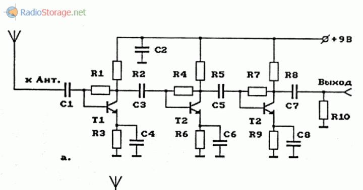
Figure 1 (a) shows broadband UHF circuit according to the common emitter circuit(OE). Depending on the transistor used, this circuit can be successfully applied up to frequencies of hundreds of megahertz.
It is necessary to recall that the reference data for transistors provides maximum frequency parameters. It is known that when assessing the frequency capabilities of a transistor for a generator, it is enough to focus on the limiting value of the operating frequency, which should be at least two to three times lower than the limiting frequency specified in the passport. However, for an RF amplifier connected according to the OE circuit, the maximum nameplate frequency must be reduced by at least an order of magnitude or more.
Fig.1. Examples of circuits of simple high-frequency (UHF) amplifiers using transistors.
Radio elements for the circuit in Fig. 1 (a):
- R1=51k (for silicon transistors), R2=470, R3=100, R4=30-100;
- C1=10-20, C2= 10-50, C3= 10-20, C4=500-Zn;
Capacitor values are given for VHF frequencies. Capacitors such as KLS, KM, KD, etc.
Transistor stages, as is known, connected in a common emitter (CE) circuit, provide relatively high gain, but their frequency properties are relatively low.
Transistor stages connected according to a common base (CB) circuit have less gain than transistor circuits with OE, but their frequency properties are better. This allows the same transistors to be used as in OE circuits, but at higher frequencies.
Figure 1 (b) shows wideband high frequency amplifier circuit (UHF) on one transistor turned on according to a common base scheme. The LC circuit is included in the collector circuit (load). Depending on the transistor used, this circuit can be successfully applied up to frequencies of hundreds of megahertz.
Radio elements for the circuit in Fig. 1 (b):
- R1=1k, R2=10k. R3=15k, R4=51 (for supply voltage ZV-5V). R4=500-3 k (for supply voltage 6V-15V);
- C1=10-20, C2=10-20, C3=1n, C4=1n-3n;
- T1 - silicon or germanium RF transistors, for example. KT315. KT3102, KT368, KT325, GT311, etc.
Capacitor and circuit values are given for VHF frequencies. Capacitors such as KLS, KM, KD, etc.
Coil L1 contains 6-8 turns of PEV 0.51 wire, brass cores 8 mm long with M3 thread, 1/3 of the turns are drained.
Figure 1 (c) shows another broadband circuit UHF on one transistor, included according to a common base scheme. An RF choke is included in the collector circuit. Depending on the transistor used, this circuit can be successfully applied up to frequencies of hundreds of megahertz.
Radioelements:
- R1=1k, R2=33k, R3=20k, R4=2k (for supply voltage 6V);
- C1=1n, C2=1n, C3=10n, C4=10n-33n;
- T1 - silicon or germanium RF transistors, for example, KT315, KT3102, KT368, KT325, GT311, etc.
The values of capacitors and circuit are given for frequencies of the MF and HF ranges. For higher frequencies, for example, for the VHF range, the capacitance values should be reduced. In this case, D01 chokes can be used.
Capacitors such as KLS, KM, KD, etc.
L1 coils are chokes; for the CB range these can be coils on rings 600NN-8-K7x4x2, 300 turns of PEL 0.1 wire.
Higher gain value can be obtained by using multi-transistor circuits. These can be various circuits, for example, made on the basis of an OK-OB cascode amplifier using transistors of different structures with serial power supply. One of the variants of such a UHF scheme is shown in Fig. 1 (d).
This UHF circuit has significant gain (tens or even hundreds of times), but cascode amplifiers cannot provide significant gain at high frequencies. Such schemes are usually used at frequencies in the LW and SV ranges. However, with the use of ultra-high frequency transistors and careful design, such circuits can be successfully applied up to frequencies of tens of megahertz.
Radioelements:
- R1=33k, R2=33k, R3=39k, R4=1k, R5=91, R6=2.2k;
- C1=10n, C2=100, C3=10n, C4=10n-33n. C5=10n;
- T1 -GT311, KT315, KT3102, KT368, KT325, etc.
- T2 -GT313, KT361, KT3107, etc.
The capacitor and circuit values are given for frequencies in the CB range. For higher frequencies, such as the HF band, capacitance values and loop inductance (number of turns) must be reduced accordingly.
Capacitors such as KLS, KM, KD, etc. Coil L1 - for the CB range contains 150 turns of PELSHO 0.1 wire on 7 mm frames, trimmers M600NN-3-SS2.8x12.
When setting up the circuit in Fig. 1 (d), it is necessary to select resistors R1, R3 so that the voltages between the emitters and collectors of the transistors become the same and amount to 3V at a circuit supply voltage of 9 V.
The use of transistor UHF makes it possible to amplify radio signals. coming from antennas, in television bands - meter and decimeter waves. In this case, antenna amplifier circuits built on the basis of circuit 1(a) are most often used.
Antenna amplifier circuit example for frequency range 150-210 MHz is shown in Fig. 2 (a).

Fig.2.2. MV antenna amplifier circuit.
Radioelements:
- R1=47k, R2=470, R3= 110, R4=47k, R5=470, R6= 110. R7=47k, R8=470, R9=110, R10=75;
- C1=15, C2=1n, C3=15, C4=22, C5=15, C6=22, C7=15, C8=22;
- T1, T2, TZ - 1T311(D,L), GT311D, GT341 or similar.
Capacitors such as KM, KD, etc. The frequency band of this antenna amplifier can be expanded in the low frequency region by a corresponding increase in the capacitances included in the circuit.
Radio elements for the antenna amplifier option for the range 50-210 MHz:
- R1=47k, R2=470, R3= 110, R4=47k, R5=470, R6= 110. R7=47k, R8=470. R9=110, R10=75;
- C 1=47, C2= 1n, C3=47, C4=68, C5=47, C6=68, C7=47, C8=68;
- T1, T2, TZ - GT311A, GT341 or similar.
Capacitors such as KM, KD, etc. When repeating this device, all requirements must be met. requirements for installation of HF structures: minimum lengths of connecting conductors, shielding, etc.
An antenna amplifier designed for use in the television signal range (and higher frequencies) can be overloaded with signals from powerful CB, HF, and VHF radio stations. Therefore, a wide frequency band may not be optimal because this may interfere with the amplifier's normal operation. This is especially true in the lower region of the amplifier's operating range.
For the circuit of the given antenna amplifier, this can be significant, because The slope of the gain decay in the lower part of the range is relatively low.
You can increase the steepness of the amplitude-frequency response (AFC) of this antenna amplifier by using 3rd order high pass filter. To do this, an additional LC circuit can be used at the input of the specified amplifier.
The connection diagram for an additional LC high-pass filter to the antenna amplifier is shown in Fig. 2(b).
Additional filter parameters (indicative):
- C=5-10;
- L - 3-5 turns PEV-2 0.6. winding diameter 4 mm.
It is advisable to adjust the frequency band and frequency response shape using appropriate measuring instruments (sweeping frequency generator, etc.). The shape of the frequency response can be adjusted by changing the values of capacitors C, C1, changing the pitch between turns L1 and the number of turns.
Using the described circuit solutions and modern high-frequency transistors (ultra-high-frequency transistors - microwave transistors), you can build an antenna amplifier for the UHF range. This amplifier can be used either with a UHF radio receiver, for example, part of a VHF radio station, or in conjunction with a TV.
Figure 3 shows UHF antenna amplifier circuit.

Fig.3. UHF antenna amplifier circuit and connection diagram.
Main parameters of the UHF range amplifier:
- Frequency band 470-790 MHz,
- Gain - 30 dB,
- Noise figure -3 dB,
- Input and output impedance - 75 Ohm,
- Current consumption - 12 mA.
One of the features of this circuit is the supply of supply voltage to the antenna amplifier circuit through the output cable, through which the output signal is supplied from the antenna amplifier to the radio signal receiver - a VHF radio receiver, for example, a VHF radio receiver or TV.
The antenna amplifier consists of two transistor stages connected in a circuit with a common emitter. A 3rd order high-pass filter is provided at the input of the antenna amplifier, limiting the range of operating frequencies from below. This increases the noise immunity of the antenna amplifier.
Radioelements:
- R1 = 150k, R2=1k, R3=75k, R4=680;
- C1=3.3, C10=10, C3=100, C4=6800, C5=100;
- T1, T2 - KT3101A-2, KT3115A-2, KT3132A-2.
- Capacitors C1, C2 are type KD-1, the rest are KM-5 or K10-17v.
- L1 - PEV-2 0.8 mm, 2.5 turns, winding diameter 4 mm.
- L2 - RF choke, 25 µH.
Figure 3 (b) shows a diagram of connecting the antenna amplifier to the antenna socket of the TV receiver (to the UHF selector) and to a remote 12 V power source. In this case, as can be seen from the diagram, power is supplied to the circuit through the coaxial cable used and for transmitting an amplified UHF radio signal from an antenna amplifier to a receiver - a VHF radio or to a TV.
Radio connection elements, Fig. 3 (b):
- C5=100;
- L3 - RF choke, 100 µH.
The installation is carried out on double-sided fiberglass SF-2 in a hinged manner, the length of the conductors and the area of the contact pads are minimal, it is necessary to provide careful shielding of the device.
Setting up the amplifier comes down to setting the collector currents of the transistors and are regulated using R1 and RЗ, T1 - 3.5 mA, T2 - 8 mA; the shape of the frequency response can be adjusted by selecting C2 within 3-10 pF and changing the pitch between turns of L1.
Literature: Rudomedov E.A., Rudometov V.E - Electronics and spy passions-3.
The amplification of received radio signals in the receiving device is carried out in its preselector, i.e. at radio frequency, and after the frequency converter - at intermediate frequency. Accordingly, a distinction is made between radio frequency amplifiers (RFA) and intermediate frequency amplifiers (IFA). In these amplifiers, along with the amplification, frequency selectivity of the receiver must be ensured. For this purpose, amplifiers contain resonant circuits: single oscillating circuits, filters on coupled circuits, various types of concentrated selectivity filters. RF amplifiers with variable tuning are usually made with a selective system similar to that used in the receiver input circuit, most often these are single-circuit selective circuits.
Complex types of selective systems with frequency response close to rectangular, such as electromechanical filters, are used in intermediate frequency amplifiers. ( EMF ), quartz filters (QF), filters based on surface (bulk) acoustic waves (SAW, SAW), etc.
Most modern receivers use single-stage amplifiers. Less commonly, with high requirements for selectivity and noise figure, AMPs can contain up to three stages.
The main electrical characteristics of amplifiers include:
1.Resonant voltage gain .
At ultrahigh frequencies (microwaves), the concept of power gain is more often used  ,
Where
,
Where  -
active component of the input conductivity of the amplifier;
-
active component of the input conductivity of the amplifier;  - active component of the load conductivity.
2.Frequency selectivity of the amplifier shows the relative reduction in gain for a given detuning  .
.
Sometimes selectivity is characterized by a squareness coefficient, for example,  .
.
3.Noise figure determines the noise properties of the amplifier.
4. Signal distortion in the amplifier: amplitude-frequency, phase, nonlinear.
5. Amplifier stability is determined by its ability to maintain basic characteristics during operation (usually K o and frequency response), as well as the absence of a tendency to self-excitation.
Figures 1-3 show the main circuits of the amplifier, and Figure 4 shows the circuit of the amplifier with a selectivity concentration filter (FSI) in the form of an electromechanical filter.

Fig.1. URCH on a field-effect transistor

Fig.2. URCH on a bipolar transistor

Fig.3. URCH with inductive coupling to the electoral system

Fig.4. Amplifier with concentrated selectivity filter
In radio frequency and intermediate frequency amplifiers, two options for connecting an amplification device are mainly used: with a common emitter (common source) and a cascode circuit for connecting transistors.
Figure 1 shows a circuit of an amplifier based on a field-effect transistor with a common source. An oscillatory circuit is included in the drain circuit L TO WITH TO . The circuit is adjusted by capacitor C TO(can be used to configure a varicap or varicap matrix circuit).
The amplifier uses serial drain power through a filter R3 C3 . Gate Bias Voltage VT1 determined by the voltage drop from the source current across the resistor R2 . Resistor R1 is the leakage resistance of the transistor VT1 and serves to transmit bias voltage to the gate of the transistor.
In Fig. Figure 2 shows a similar circuit of the RF amplifier based on a bipolar transistor. Here, double incomplete inclusion of the circuit with transistors VT1, VT2, which makes it possible to provide the necessary bypassing of the circuit from the output side of transistor VT1 and from the input side of transistor VT2 . The supply voltage is supplied to the transistor collector through filter R4C4 and part of the circuit coil turns L TO . DC mode and temperature stabilization are provided using resistors R1, R2 and R3. Capacity C2 Eliminates negative AC feedback.
In Fig. Figure 3 shows a circuit with a transformer connection of the circuit to the transistor collector and an autotransformer connection to the input of the next stage. Usually, in this case, an “extended” circuit setting is used (see laboratory work No. 1).
In Fig. Figure 4 shows a diagram of an amplifier cascade with FSI, made on a 265 UVZ chip . The microcircuit is a cascode amplifier OE - OB.
Intermediate frequency amplifiers provide the receiver's main gain and adjacent channel selectivity. Their important feature is that they operate at a fixed intermediate frequency and have a high gain of the order of  .
.
When using various types of FSI, the required amplifier gain is achieved by using broadband cascades.
Common to all schemes is the double incomplete inclusion of the electoral system. (Full inclusion can be considered as a special case when the transformation coefficients m and n are equal to one). Therefore, for analysis you can use one generalized equivalent equivalent circuit of the amplifier (see Fig. 5).

Fig.5. Generalized equivalent circuit of a resonant amplifier
In the diagram, the transistor on the output side is replaced by an equivalent current generator with the parameters  ,
, and electric shock
  , and from the input side of the next stage the conductivity
  ,
, . Leakage resistor R4 (Fig. 1) or divider
  (Fig. 2) are replaced by conductivity
  (
( or
or  ).
).
Usually the sum of conductivities  considered to be the load conductivity GN, i.e.
Analysis of the equivalent circuit allows us to obtain all the calculated relationships for determining the characteristics of the cascade.
Thus, the complex gain of the cascade is determined by the expression
 , Where -
equivalent resonant conductivity of the circuit;
Generalized contour detuning.
From this relationship it is easy to determine the coefficient modulus
gain

and resonant gain of the RF amplifier cascade
The resonant gain reaches its maximum value with the same shunting of the circuit from the output side of the active device and from the load side (input of the next stage), i.e. When 
The given relations allow us to obtain the equation of the amplifier's resonance curve. So, with small detunes,  . From where, RF bandwidth
level 0.707 (- 3dB) is equal to
. From where, RF bandwidth
level 0.707 (- 3dB) is equal to
The resonant gain of the single-circuit amplifier cascade is the same as that of the single-circuit amplifier
For an amplifier with a two-circuit bandpass filter, the resonant gain of the cascade is determined by the expression
Where  -
factor of connection between circuits, and
-
factor of connection between circuits, and  - coupling coefficient between circuits.
The gain (voltage) of an amplifier with any FSI when matching the filter at the input and output can be calculated using the formula
Here  ,
, - characteristic (wave) impedances of the FSI at the input and output, respectively;
 - transmission coefficient of the filter in the transparency (transmission) band.
In the event that the attenuation of the filter in the transparency band is known  V
decibels, then
V
decibels, then
Inclusion factors m And n are calculated from the filter matching condition at the input and output
 ,
,
 .
.
The resonant characteristic of the amplifier cascade with FSI is completely determined by the transmission coefficient change curve FSI from frequency. Individual points of the resonance curve FSI are given in reference books.
The gain of the selective amplifier should not exceed the value of the stable gain  . In general,
  can be estimated from the expression

If a cascode circuit is used as an amplifying element, then it is necessary to substitute the corresponding conductance values for the cascode circuit, for example, for the OE - OB circuit

In the case of using field-effect transistors, the active component of conductivity can be neglected
 .
.
URFs are active frequency-selective cascades of receivers operating at a fixed frequency or in a frequency range. They are used to ensure high sensitivity of radio receiving devices due to preliminary amplification of the signal and its frequency selection.
Basic requirements and quality indicators
1. Resonant voltage gain
Or by power
Where G in, G n - active components of the input and load conductances of the amplifier.
2. Frequency selectivity- mainly through the mirror channel of superheterodyne receivers (  ).
).
3. Noise figure of the RF frequency control, which largely determines the receiver’s ability to reproduce useful information at low levels of the received signal. From the point of view of the minimum noise level, it is enough for the power gain of the RF amplifier to be at the level of 10-100, so the required number of stages usually does not exceed two.
4. Sustainability, characterizes the absence of self-excitation of the amplifier.
In addition, according to their performance, the RF amplifiers must provide signal amplification in a certain dynamic range with distortion not exceeding a specified level.
Considering that the RF amplifier operates in the mode of amplifying weak signals, we will consider the amplifier device to be a linear active 4-pole network.
Resonant mid-high frequency amplifier stage
In the moderately high frequency range ( f < 300 MHz) to describe the properties of amplifier stages it is convenient to use the system Y-parameters, in which the equation of a linear 4-port network is written in the form (5.1)
 (5.1)
(5.1)
Where  ,
,
 And
And  ,
, -
voltages and currents at the input and output of the 4-port network, respectively,
-
voltages and currents at the input and output of the 4-port network, respectively,
 - parameters in short circuit mode at the input and output of a 4-pole network.
The most general circuit of a resonant cascade can be presented as (Fig. 5.1).

The figure shows a circuit of a resonant amplifier, in which to the circuit LC partially connected as transistor output VT 1, so the input of the next stage on the transistor VT 2 . In both cases, autotransformer coupling is used. However, in such an amplifier, these connections can be implemented in another known way, for example, using a transformer.
Elements R 1 ,
R 2 ,
,
 used to set the operating mode of the active element VT 1
by direct current. The necessary filtering for power supply is carried out by a filter R f ,
C f .
The calculation of these elements is carried out in the same way as is done for aperiodic amplifiers. Therefore, issues of setting the operating point of resonant amplifiers are not considered here.
used to set the operating mode of the active element VT 1
by direct current. The necessary filtering for power supply is carried out by a filter R f ,
C f .
The calculation of these elements is carried out in the same way as is done for aperiodic amplifiers. Therefore, issues of setting the operating point of resonant amplifiers are not considered here.

From the presented equivalent circuit it follows that
 (5.2)
(5.2)
When using double autotransformer coupling, the load conductivity can be represented as
 , (5.3)
Where,  .
.
The voltage gain can be obtained by using expressions (5.1) and (5.2). Taking these expressions into account, we can obtain
 (5.4)
(5.4)
From the last expression we can get
 (5.5)
(5.5)
Where do we get it from?
 , (5.6)
where is the total equivalent conductivity of the circuit.
The resonant properties of the cascade are determined by the frequency response of the conductivity  ,
and the latter corresponds to the resonant characteristic of the oscillatory circuit L.C..
The equivalent resistance of the oscillatory circuit included in the collector circuit of the transistor can be represented as follows
,
and the latter corresponds to the resonant characteristic of the oscillatory circuit L.C..
The equivalent resistance of the oscillatory circuit included in the collector circuit of the transistor can be represented as follows
Total equivalent loop resistance  one can imagine
 , (5.8)
Where  -generalized contour detuning.
The cascade gain at the resonant frequency can be represented as
 , (5.9)
Where  .
.
 - transformation coefficient from the output of the first active element to the input of the next one.
Taking this into account for the resonant cascade, we obtain the following expression for the gain
 (5.10)
In structure, the resulting formula corresponds to the formula for determining the gain of an aperiodic cascade, only a resonant circuit is used as a load in the latter.
Current consumption - 46 mA. The bias voltage V bjas determines the output power level (gain) of the amplifier

Fig. 33.11. Internal structure and pinout of TSH690, TSH691 microcircuits

Rice. 33.12. Typical inclusion of TSH690, TSH691 microcircuits as an amplifier in the frequency band 300-7000 MHz
and can be adjusted within 0-5.5 (6.0) V. The transmission coefficient of the TSH690 (TSH691) microcircuit at a bias voltage V bias = 2.7 V and a load resistance of 50 Ohms in a frequency band up to 450 MHz is 23 (43) dB, up to 900(950) MHz - 17(23) dB.
Practical inclusion of TSH690, TSH691 microcircuits is shown in Fig. 33.12. Recommended element values: C1=C5=100-1000 pF; C2=C4=1000 pF; C3=0.01 µF; L1 150 nH; L2 56 nH for frequencies not exceeding 450 MHz and 10 nH for frequencies up to 900 MHz. Resistor R1 can be used to regulate the output power level (can be used for an automatic output power control system).
The broadband INA50311 (Fig. 33.13), manufactured by Hewlett Packard, is intended for use in mobile communications equipment, as well as in consumer electronic equipment, for example, as an antenna amplifier or radio frequency amplifier. The operating range of the amplifier is 50-2500 MHz. Supply voltage - 5 V with current consumption up to 17 mA. Average gain

Rice. 33.13. internal structure of the ΙΝΑ50311 microcircuit
10 dB. The maximum signal power supplied to the input at a frequency of 900 MHz is no more than 10 mW. Noise figure 3.4 dB.
A typical connection of the ΙΝΑ50311 microcircuit when powered by a 78LO05 voltage stabilizer is shown in Fig. 33.14.

Rice. 33.14. broadband amplifier on the INA50311 chip
Shustov M. A., Circuitry. 500 devices on analog chips. - St. Petersburg: Science and Technology, 2013. -352 p.
Good afternoon, dear Habrauser, I want to tell you about the basics of building audio amplifiers. I think this article will be interesting to you if you have never worked in radio electronics, and of course it will be funny to those who never part with a soldering iron. And so I will try to talk about this topic as simply as possible and, unfortunately, omitting some of the nuances.An audio amplifier or low frequency amplifier, in order to understand how it works and why there are so many transistors, resistors and capacitors, you need to understand how each element works and try to find out how these elements are arranged. In order to assemble a primitive amplifier, we will need three types of electronic elements: resistors, capacitors and, of course, transistors.
Resistor
So, our resistors are characterized by resistance to electric current and this resistance is measured in Ohms. Each electrically conductive metal or metal alloy has its own resistivity. If we take a wire of a certain length with a high resistivity, then we will get a real wirewound resistor. To make the resistor compact, the wire can be wound around the frame. This way we get a wirewound resistor, but it has a number of disadvantages, so resistors are usually made of metal-ceramic material. This is how resistors are designated on electrical diagrams:The upper version of the designation is adopted in the USA, the lower one in Russia and Europe.
Capacitor
A capacitor consists of two metal plates separated by a dielectric. If we apply a constant voltage to these plates, an electric field will appear, which, after turning off the power, will maintain positive and negative charges on the plates, respectively.
The basis of the capacitor design is two conductive plates, between which there is a dielectric
In this way, the capacitor is able to accumulate electrical charge. This ability to accumulate electrical charge is called electrical capacitance, which is the main parameter of a capacitor. Electrical capacitance is measured in Farads. What is also characteristic is that when we charge or discharge a capacitor, an electric current flows through it. But as soon as the capacitor is charged, it stops passing electric current, and this is because the capacitor has accepted the charge of the power source, that is, the potential of the capacitor and the power source are the same, and if there is no potential difference (voltage), there is no electric current. Thus, a charged capacitor does not pass direct electric current, but does allow alternating current, since when connected to an alternating electric current, it will be constantly charged and discharged. On electrical diagrams it is designated as follows:

Transistor
In our amplifier we will use the simplest bipolar transistors. A transistor is made from a semiconductor material. The property we need of this material is the presence in them of free carriers of both positive and negative charges. Depending on which charges are greater, semiconductors are divided into two types according to conductivity: n-type and p-type (n-negative, p-positive). Negative charges are electrons released from the outer shells of atoms in the crystal lattice, and positive charges are so-called holes. Holes are vacant spaces remaining in electron shells after electrons leave them. Conventionally, we denote atoms with an electron in the outer orbit by a blue circle with a minus sign, and atoms with a vacant place by an empty circle:
Each bipolar transistor consists of three zones of such semiconductors, these zones are called base, emitter and collector.

Let's look at an example of how a transistor works. To do this, connect two 1.5 and 5 volt batteries to the transistor, with the plus to the emitter and the minus to the base and collector, respectively (see figure):

An electromagnetic field will appear at the contact between the base and emitter, which literally pulls out electrons from the outer orbit of the base atoms and transfers them to the emitter. Free electrons leave behind holes and occupy vacant places already in the emitter. This same electromagnetic field has the same effect on the atoms of the collector, and since the base in the transistor is quite thin relative to the emitter and collector, the collector electrons quite easily pass through it to the emitter, and in much greater quantities than from the base.
If we turn off the voltage from the base, then there will be no electromagnetic field, and the base will act as a dielectric, and the transistor will be closed. Thus, by applying a sufficiently low voltage to the base, we can control the higher voltage applied to the emitter and collector.
The transistor we considered pnp-type, since he has two p-zones and one n-zone. There are also npn-transistors, the principle of operation in them is the same, but the electric current flows in them in the opposite direction than in the transistor we considered. This is how bipolar transistors are indicated on electrical diagrams, the arrow indicates the direction of the current: 
ULF
Well, let's try to design a low-frequency amplifier from all this. First, we need a signal that we will amplify; it can be a computer sound card or any other audio device with a linear output. Let's say our signal with a maximum amplitude of approximately 0.5 volts at a current of 0.2 A, something like this:
And in order for the simplest 4-ohm 10-watt speaker to work, we need to increase the signal amplitude to 6 volts, at current strength I = U / R= 6 / 4 = 1.5 A.
So, let's try to connect our signal to a transistor. Remember our circuit with a transistor and two batteries, now instead of a 1.5 volt battery we have a line output signal. Resistor R1 acts as a load so that there is no short circuit and our transistor does not burn out.

But here two problems arise at once, firstly our transistor npn-type, and opens only when the half-wave value is positive, and closes when the half-wave is negative.

Secondly, a transistor, like any semiconductor device, has nonlinear characteristics in terms of voltage and current, and the lower the current and voltage values, the stronger these distortions:

Not only is there only a half-wave left of our signal, but it will also be distorted:

This is the so-called step-type distortion.
To get rid of these problems, we need to shift our signal to the working area of the transistor, where the entire sinusoid of the signal will fit and nonlinear distortions will be negligible. To do this, a bias voltage, say 1 volt, is applied to the base using a voltage divider made up of two resistors R2 and R3.

And our signal entering the transistor will look like this:

Now we need to remove our useful signal from the collector of the transistor. To do this, install capacitor C1:

As we remember, a capacitor allows alternating current to pass through and does not allow direct current to pass through, so it will serve as a filter that passes only our useful signal - our sine wave. And the constant component that has not passed through the capacitor will be dissipated by resistor R1. Alternating current, our useful signal, will tend to pass through the capacitor, so the resistance of the capacitor for it is negligible compared to resistor R1.
This is the first transistor stage of our amplifier. But there are two more small nuances:
We don’t know 100% what signal is entering the amplifier, what if the signal source is faulty, anything can happen, again static electricity or a constant voltage passes along with the useful signal. This may cause the transistor to not work properly or even cause it to break. To do this, we will install capacitor C2; like capacitor C1, it will block direct electric current, and the limited capacitance of the capacitor will not allow large amplitude peaks to pass through, which can damage the transistor. These power surges usually occur when the device is turned on or off.

And the second nuance is that any signal source requires a certain specific load (resistance). Therefore, the input impedance of the cascade is important for us. To adjust the input resistance, add resistor R4 to the emitter circuit:

Now we know the purpose of each resistor and capacitor in the transistor stage. Let's now try to calculate what element values need to be used for it.
Initial data:
- U= 12 V - supply voltage;
- U bae~ 1 V - Emitter-base voltage of the transistor operating point;

- Pmax= 200 mW - maximum power dissipation;
- Imax= 100 mA - maximum constant collector current;
- Umax= 18 V - maximum permissible voltage collector-base / collector-emitter (We have a supply voltage of 12 V, so there is enough to spare);
- U eb= 5 V - maximum permissible emitter-base voltage (our voltage is 1 volt ± 0.5 volt);
- h21= 75-225 - base current amplification factor, the minimum value is accepted - 75;
- We calculate the maximum static power of the transistor, it is taken 20% less than the maximum power dissipation, so that our transistor does not work at the limit of its capabilities:
P st.max = 0,8*Pmax= 0.8 * 200mW = 160 mW;
- Let's determine the collector current in static mode (without a signal), despite the fact that no voltage is supplied to the base through the transistor, electric current still flows to a small extent.
I k0 =P st.max / U ke, Where U ke- collector-emitter junction voltage. Half of the supply voltage is dissipated on the transistor, the second half will be dissipated on resistors:
U ke = U / 2;
I k0 = P st.max / (U/ 2) = 160 mW / (12V / 2) = 26.7 mA;
- Now let's calculate the load resistance, initially we had one resistor R1, which performed this role, but since we added resistor R4 to increase the input resistance of the cascade, now the load resistance will be the sum of R1 and R4:
R n = R1 + R4, Where R n- total load resistance;
The ratio between R1 and R4 is usually taken to be 1 to 10:
R1 =R4*10;
Let's calculate the load resistance:
R1 + R4 = (U / 2) / I k0= (12V / 2) / 26.7 mA = (12V / 2) / 0.0267 A = 224.7 Ohm;
The closest resistor values are 200 and 27 Ohms. R1= 200 Ohm, a R4= 27 Ohm.
- Now let’s find the voltage at the collector of the transistor without a signal:
U k0 = (U ke0 + I k0 * R4) = (U - I k0 * R1) = (12V -0.0267 A * 200 Ohm) = 6.7 V;
- Transistor control base current:
I b = I to / h21, Where I to- collector current;
I to = (U / R n);
I b = (U / R n) / h21= (12V / (200 Ohm + 27 Ohm)) / 75 = 0.0007 A = 0.07 mA;
- The total base current is determined by the base bias voltage, which is set by the divider R2 And R3. The current specified by the divider should be 5-10 times greater than the base control current ( I b), so that the base control current itself does not affect the bias voltage. Thus, for the current divider value ( I cases) we accept 0.7 mA and calculate R2 And R3:
R2 + R3 = U / I cases= 12V / 0.007 = 1714.3 Ohm
- Now let's calculate the voltage at the emitter at rest of the transistor ( U e):
U e = I k0 * R4= 0.0267 A * 27 Ohm = 0.72 V
Yes, I k0 collector quiescent current, but the same current also passes through the emitter, so I k0 is considered the quiescent current of the entire transistor.
- We calculate the total voltage at the base ( U b) taking into account the bias voltage ( U cm= 1V):
U b = U e + U cm= 0.72 + 1 = 1.72 V
Now, using the voltage divider formula, we find the resistor values R2 And R3:
R3 = (R2 + R3) * U b / U= 1714.3 Ohm * 1.72 V / 12 V = 245.7 Ohm;
The closest resistor value is 250 ohms;
R2 = (R2 + R3) - R3= 1714.3 Ohm - 250 Ohm = 1464.3 Ohm;
We select the resistor value in the direction of decrease, the closest R2= 1.3 kOhm.
- Capacitors C1 And C2 Usually set to at least 5 µF. The capacitance is chosen such that the capacitor does not have time to recharge.
Conclusion
At the output of the cascade, we receive a proportionally amplified signal in both current and voltage, that is, in power. But one stage is not enough for us to achieve the required gain, so we will have to add the next and the next... And so on.The considered calculation is quite superficial and such an amplification circuit, of course, is not used in the construction of amplifiers; we must not forget about the range of transmitted frequencies, distortion and much more.