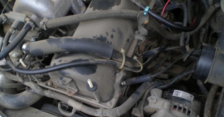
Perhaps the most difficult part of the amplifier design is to power the subwoofer channel from the on-board 12 volt network. There are a lot of reviews about it in various forums, but it’s very difficult to make a really good converter on the advice of experts, see for yourself when it comes to this part of the design. To do this, I decided to focus on the assembly of the voltage converter, perhaps this will be the most detailed description, since it sets out a two-week work, as the people say - from<<А>> before<<Я>>.
There are a lot of voltage converter circuits, but as a matter of fact, after assembly, defects, malfunctions, incomprehensible overheating of individual parts and parts of the circuit appear. The assembly of the converter dragged on for two weeks, since a number of changes were made to the main circuit, as a result, I can safely say that it turned out to be a powerful and reliable converter.
The main task was to build a 300-350 watt converter to power the amplifier according to the Lanzar circuit, everything turned out nice and neat, everything except the board, we have a big shortage of chemistry for etching the boards, so I had to use a breadboard, but I don’t advise repeating my torment, soldering wiring for each track, tinning each hole and contact is not an easy job, you can judge this by looking at the board from the back. For a beautiful appearance, a wide green adhesive tape was glued to the board.
PULSE TRANSFORMER
The main change in the circuit is the pulse transformer. In almost all articles on homemade subwoofer installations, the transformer is made on ferrite rings, but rings are sometimes not available (as in my case). The only thing was an alsifer ring from a high-frequency choke, but the operating frequency of this ring did not allow it to be used as a transformer in a voltage converter.

Here I was lucky, almost for nothing I got a pair of computer power supplies, fortunately in both blocks there were completely identical transformers.

As a result, it was decided to use two transformers as one, although one such transformer can provide the desired power, but when winding the windings, they simply would not fit, so it was decided to redo both transformers.

In the beginning, you need to remove the hearts, in fact, the work is quite simple. We heat the ferrite stick with a lighter, which closes the main heart and after 30 seconds of heat, the glue melts and the ferrite stick falls out. From overheating, the properties of the stick may change, but this is not so important, since we will not use sticks in the main transformer.

We do the same with the second transformer, then we remove all the standard windings, clean the transformer leads and cut off one of the side walls of both transformers, it is advisable to cut off the wall free from contacts.

The next part of the work is gluing the frames. The attachment point (seam) can simply be wrapped with electrical tape or tape, I do not recommend using a variety of adhesives, as this may interfere with the insertion of the core.

I had experience in assembling voltage converters, but nevertheless this converter survived all the juice and money from me, since 8 field workers were killed during the work and the transformer was to blame for everything.
Experiments with the number of turns, winding technology and wire cross-section led to pleasing results.
So the most difficult thing is winding. Many forums advise winding a thick primary, but experience has shown that it doesn’t take much to get the indicated power. The primary winding consists of two completely identical windings, each of them is wound with 5 strands of 0.8 mm wire, stretched along the entire length of the frame, but we will not rush. To begin with, we take a wire with a diameter of 0.8 mm, the wire is preferably new and even, without bends (although I used the wire from the network winding of the same transformers from power supplies).

Next, we wind 5 turns along one wire along the entire length of the transformer frame (you can also wind all the wires together with a bundle). After winding the first core, it needs to be strengthened by simply winding it onto the side terminals of the transformer. After that, we already wind the rest of the cores, evenly and neatly. After winding is completed, you need to get rid of the varnish coating at the ends of the winding, this can be done in several ways - heat the wires with a powerful soldering iron or peel off the varnish individually from each wire with a mounting knife or razor. After that, you need to tin the ends of the wires, weave them into a pigtail (it is convenient to use pliers) and cover with a thick layer of tin.
After that, we move on to the second half of the primary winding. It is completely identical with the first one; before winding it, we cover the first part of the winding with electrical tape. The second half of the primary winding is also stretched over the entire frame and wound in the same direction as the first, we wind it according to the same principle, one strand.

After winding is completed, the windings must be phased. We should get one winding, which consists of 10 turns and has a tap from the middle. It is important to remember one important detail here - the end of the first half should join with the beginning of the second half, or vice versa, so that there are no difficulties in phasing, it is better to do everything from photographs.
After hard work, the primary winding is finally ready! (you can drink beer).
The secondary winding also requires a lot of attention, since it is it that will feed the power amplifier. It is wound according to the same principle as the primary one, only each half consists of 12 turns, which completely provides a bipolar voltage of 50-55 volts at the output.

The winding consists of two halves, each is wound with 3 cores of 0.8 mm wire, the wires are stretched throughout the frame. After winding the first half, we isolate the winding and wind the second half on top in the same direction as the first. As a result, we get two identical halves, which are phased in the same way as the primary. After the conclusions are cleaned, weaved and soldered to each other.

One important point - if you decide to use other types of transformers, then make sure that the halves of the heart do not have a gap, as a result of experiments, it was found that even the slightest gap of 0.1 mm sharply disrupts the operation of the circuit, the current consumption increases by 3-4 times , field-effect transistors begin to overheat so that the cooler does not have time to cool them.

The finished transformer can be shielded with copper foil, but this does not play a particularly big role.

The result is a compact transformer that can easily deliver the required power.
The device diagram is not simple, I do not advise novice radio amateurs to contact him. The basis, as always, is a pulse generator built on an integrated circuit TL494. An additional output amplifier is built on a pair of low-power transistors of the BC 557 series, an almost complete analogue of the BC556; KT3107 can be used from a domestic interior. As power switches, two pairs of powerful field-effect transistors of the IRF3205 series are used, 2 field switches per shoulder.

Transistors are installed on small heat sinks from computer power supplies, insulated from the heat sink with a special gasket.
The 51 ohm resistor is the only part of the circuit that overheats, so a 2 watt resistor is needed (although I only have 1 watt), but overheating is not terrible, it does not affect the operation of the circuit in any way.
Mounting, especially on a breadboard, is a very tedious process, so it's best to do everything on a printed circuit board. We make the plus and minus tracks wider, then we cover them with thick layers of tin, since a considerable current will flow through them, the same thing with the drains of field workers.
We put 22 ohm resistors on 0.5-1 watt, they are designed to remove overload from the microcircuit.

The limiting resistors of the gate current of the field workers and the limiting resistor of the supply current of the microcircuit (10 ohms) are preferably half a watt, all other resistors can be 0.125 watts.

The frequency of the converter is set using a 1.2nf capacitor and a 15k resistor, by reducing the capacitance of the capacitor and increasing the resistance of the resistor, you can raise the frequency or vice versa, but it is advisable not to play with the frequency, since the operation of the entire circuit may be disrupted.
Rectifier diodes were used by the KD213A series, they did the best job, because due to the operating frequency (100 kHz) they felt great, although you can use any high-speed diodes with a current of at least 10 amperes, it is also possible to use Schottky diode assemblies, which can be found in the same computer power supplies, in one case there are 2 diodes that have a common cathode, so for a diode bridge you will need 3 such diode assemblies. Another diode is installed to power the circuit, this diode serves as protection against power reversal.

Unfortunately, I have capacitors with a voltage of 35 volts 3300 microfarads, but it is better to choose a voltage from 50 to 63 volts. There are two such capacitors on the shoulder.
The circuit uses 3 chokes, the first to power the converter circuit. This choke can be wound on standard yellow rings from power supplies. We wind 10 turns evenly around the entire ring, the wire into two strands of 1 mm each.


Chokes for filtering high-frequency interference after the transformer also contain 10 turns, a wire with a diameter of 1-1.5 mm, wound on the same rings or on ferrite rods of any brand (rod diameter is not critical, length 2-4 cm).
Power is supplied to the converter when the Remote Control (REM) wire is shorted to the power plus, this closes the relay and the converter starts to work. I used two relays connected in parallel for 25 amps each.

The coolers are soldered to the converter unit and turn on immediately after the REM wire is turned on, one of them is designed to cool the converter, the other for the amplifier, you can also install one of the coolers in the opposite direction so that the latter removes warm air from the common case.
RESULTS AND COSTS
Well, what can I say, the converter justified all the hopes and costs, it works like a clock. As a result of the experiments, he was able to give an honest 500 watts and could have done more if the diode bridge of the block that fed the converter had not died.
The total amount spent on the converter (prices are for the total number of parts, not just one)
IRF3205 4pcs - 5$
TL494 1pc -0.5$
BC557 3pcs - 1$
KD213A 4pcs - 4$
Capacitors 35v 3300uF 4pcs - 3$
Resistor 51ohm 1pc - $0.1
Resistor 22ohm 2pcs -0.15$
Breadboard - 1$


From this list, diodes and capacitors were given for nothing, I think, except for field workers and microcircuits, everything can be found in the attic, asked from friends or in workshops, so the price of the converter does not exceed $ 10. You can buy a ready-made Chinese amplifier for a subwoofer with all the amenities for $80-100, and goods from well-known companies cost a lot, from $300 to $1000, in return you can assemble an amplifier of identical quality for only $50-60 even less if you know where to get the parts I hope I was able to answer many questions.
Currently, a huge range of radio tape recorders of different price categories is presented on the automotive equipment market. Modern car radios usually have 4 line outputs (some still have a separate subwoofer output). They are designed to be used "head" with external power amplifiers.
Many radio amateurs make power amplifiers with their own hands. The most difficult part in a car amplifier is the voltage converter (PV). In this article, we will consider the principle of building stabilized PNs based on the already "popular" TL494 microcircuit (our analogue of KR1114EU4).
Control node
Here we will take a very detailed look at the operation of the TL494 in stabilization mode.
The sawtooth voltage generator G1 serves as the master. Its frequency depends on the external elements of C3R8 and is determined by the formula: F=1/(C3R8), where F is the frequency in Hz; C3- in Farads; R8- in ohms. When operating in a push-pull mode (our PN will just work in this mode), the frequency of the self-oscillator of the microcircuit should be two times higher than the frequency at the output of the PN. For the ratings of the timing circuit indicated on the diagram, the generator frequency F = 1 / (0.000000001 * 15000) = 66.6 kHz. The output pulse frequency is roughly 33 kHz. The generated voltage is supplied to 2 comparators (A3 and A4), the output pulses of which are summarized by the OR element D1. Further, the pulses through the elements OR - NOT D5 and D6 are fed to the output transistors of the microcircuit (VT1 and VT2). Pulses from the output of the element D1 also arrive at the counting input of the trigger D2, and each of them changes the state of the trigger. Thus, if a logical “1” is applied to pin 13 of the microcircuit (as in our case, + is applied to pin 13 from pin 14), then the pulses at the outputs of elements D5 and D6 alternate, which is necessary to control a push-pull inverter. If the microcircuit is used in a single-cycle Pn, pin 13 is connected to a common wire, as a result, trigger D2 is no longer involved in the work, and pulses appear at all outputs simultaneously.
Element A1 is an error signal amplifier in the output voltage stabilization circuit PN. This voltage is applied to pin 1 of node A1. On the second output, there is an exemplary voltage obtained from the A5 stabilizer built into the microcircuit using a resistive divider R2R3. The voltage at the output A1, proportional to the difference between the input, sets the threshold for the operation of the comparator A4 and, consequently, the duty cycle of the pulses at its output. The R4C1 chain is necessary for the stability of the stabilizer.
Transistor optocoupler U1 provides galvanic isolation in the negative voltage feedback circuit. It refers to the output voltage stabilization circuit. Also, the stabilizer of the parallel type DD1 (TL431 or our analogue KR142EN19A) is responsible for stabilization.
The voltage drop across resistor R13 is approximately 2.5 volts. The resistance of this resistor is calculated by setting the current through the resistive divider R12R13. The resistance of the resistor R12 is calculated by the formula: R12 \u003d (Uout-2.5) / I "where Uout is the output voltage of the PN; I" is the current through the resistive divider R12R13.
The load DD1 is a parallel-connected ballast resistor R11 and a radiating diode (pin 1.2 of the optocoupler U1) with a current-limiting resistor R10. The ballast resistor creates the minimum load necessary for the normal functioning of the microcircuit.
IMPORTANT. It should be taken into account that the operating voltage of the TL431 should not exceed 36 volts (see the datasheet on the TL431). If it is planned to manufacture a PN with Uout.> 35 volts, then the stabilization circuit will need to be changed a little, as will be discussed below.
Suppose that the PN is designed for an output voltage of + -35 Volts. When this voltage is reached (on pin 1 of DD1, the voltage reaches a threshold of 2.5 Volts), the stabilizer DD1 “opens”, the LED of the optocoupler U1 lights up, which will open its transistor junction. At pin 1 of the TL494 chip, the level "1" will appear. The supply of output pulses will stop, the output voltage will begin to fall until the voltage at pin 1 of the TL431 is below the threshold 2.5 Volts. As soon as this happens, DD1 "closes", the LED of the optocoupler U1 goes out, a low level appears at pin 1 of the TL494 and node A1 allows the output pulses to be sent. The output voltage will again reach +35 Volts. Again, DD1 will “open”, the LED of the optocoupler U1 will light up, and so on. This is called "duty cycle" - when the pulse frequency is unchanged, and the adjustment is carried out by pauses between pulses.
The second error signal amplifier (A2) in this case is used as an input for emergency protection. This can be a control unit for the maximum heat sink temperature of the output transistors, a UMZCH protection unit against current overload, and so on. As in A1, through the resistive divider R6R7, the reference voltage is applied to pin 15. Pin 16 will have a “0” level, since it is connected to the common wire through resistor R9. If you apply the level "1" to output 16, then node A2 will instantly disable the supply of output pulses. The PN will “stop” and start only when the level “0” appears again at the 16th output.
The function of comparator A3 is to ensure that there is a pause between pulses at the output of element D1., even if the output voltage of amplifier A1 is out of range. The minimum response threshold A3 (when pin 4 is connected to a common wire) is set by the internal voltage source GI1. With an increase in the voltage at pin 4, the minimum duration of the pause increases, therefore, the maximum output voltage of the PS decreases.
This property is used for soft start PN. The fact is that at the initial moment of operation of the PN, the capacitors of the filters of its rectifier are completely discharged, which is equivalent to closing the outputs to a common wire. Starting the PN immediately at full power will lead to a huge overload of the transistors of the powerful cascade and their possible failure. The C2R5 circuit provides a smooth, overload-free start-up of the PN.
At the first moment after switching on, C2 is discharged., And the voltage at pin 4 of TL494 is close to +5 Volts received from the A5 stabilizer. This guarantees a pause of the maximum possible duration, up to the complete absence of pulses at the output of the microcircuit. As the capacitor C2 is charged through the resistor R5, the voltage at pin 4 decreases, and with it the duration of the pause. At the same time, the output voltage of the PN increases. This continues until it approaches the exemplary one and the stabilizing feedback comes into effect, the principle of which was described above. Further charging of the capacitor C2 does not affect the processes in Stump.
As already mentioned here, the operating voltage of the TL431 should not exceed 36 volts. But what if it is required to receive, for example, 50 volts from the PN? Make it simple. It is enough to put a 15 ... 20 Volt zener diode into the break of the controlled positive wire (shown in red). As a result of this, it will “cut off” the excess voltage (if a 15-volt zener diode, then it will cut off 15 volts, if a twenty-volt one, then it will accordingly remove 20 volts) and the TL431 will operate in an acceptable voltage mode.
Based on the foregoing, a PN was built, the scheme of which is shown in the figure below.

An intermediate stage is assembled on VT1-VT4R18-R21. The task of this node is to amplify the pulses before they are fed to powerful field-effect transistors VT5-VT8.
The REM control unit is made on VT11VT12R28R33-R36VD2C24. When a control signal from the radio +12 Volts is applied to "REM IN", the transistor opens VT12, which in turn opens VT11. A voltage appears on the VD2 diode, which will power the TL494 chip. Mon starts. If the radio is turned off, then these transistors will close, the voltage converter will “stop”.
On the elements VT9VT10R29-R32R39VD5C22C23, an emergency protection unit is made. When a negative pulse is applied to the PROTECT IN input, the PN will turn off. It will be possible to start it only by re-disabling and enabling REM. If this node is not planned to be used, then the elements related to it will need to be excluded from the circuit, and pin 16 of the TL494 chip will be connected to a common wire.
In our case, the PN is bipolar. Stabilization in it is carried out according to the positive output voltage. So that there is no difference in output voltages, the so-called "DGS" is used - a group stabilization choke (L3). Both of its windings are wound simultaneously on one common magnetic circuit. Get a choke-transformer. The connection of its windings has a certain rule - they must be turned on in the opposite direction. In the diagram, the beginnings of these windings are shown with dots. As a result of this inductor, the output voltages of both arms are equalized.
Before switching on, it is necessary to check the quality of the installation. To establish a PN, a transformer power supply unit with a capacity of about 20 Amperes and with an output voltage regulation limit of 10 ... 16 Volts is required. It is not recommended to power the PN from a computer power supply.
Before turning on, you need to set the output voltage of the power supply to 12 volts. In parallel with the output of the PN, connect resistors for 2 W 3.3 kOhm both to the positive shoulder and to the negative one. Unsolder the PN resistor R3. Apply power supply from the PSU to the PN (12 Volts). Mon should not start. Next, you should apply a plus to the REM input (put a temporary jumper on the + and REM terminals). If the parts are in good condition and the installation is done correctly, then the PN should start. Next, you need to measure the current consumption (ammeter in the gap of the positive wire). The current must be within 300 ... 400 mA. If it is very different upwards, then this indicates that the circuit does not work correctly. There are many reasons, one of the main ones is the transformer is not wound correctly. If everything is within acceptable limits, then you need to measure the output voltage both positively and negatively. They should be almost the same. The result is memorized or written down. Next, in place of R3, you need to solder a series chain of a constant resistor of 27 kOhm and a trimmer (can be variable) of 10 kOhm, not forgetting to first turn off the power from the PN. Let's start PN again. After starting, we increase the voltage on the power supply to 14.4 volts. We measure the output voltage of the PN in the same way as during the initial switch-on. By rotating the axis of the tuning resistor, you need to set the output voltage, which was when the power supply was from 12 volts. After turning off the PSU, unsolder the series resistor circuit and measure the total resistance. In place of R3, solder a constant resistor of the same rating. We do a control check.
The second option for building stabilization
The figure below shows another option for building stabilization. In this circuit, not its internal stabilizer is used as a reference voltage for pin 1 of the TL494, but an external one, made on the TL431 parallel type stabilizer. Chip DD1 stabilizes the voltage of 8 volts to power the divider, consisting of a phototransistor optocoupler U1.1 and resistor R7. The voltage from the middle point of the divider is supplied to the non-inverting input of the first error signal amplifier of the TL494 SHI controller. The output voltage of the PN also depends on the resistor R7 - the lower the resistance, the lower the output voltage. The PN setting according to this scheme does not differ from the one in Figure No. 1. The only difference is that initially you need to set 8 volts at pin 3 of DD1 using the selection of resistor R1.

The voltage converter circuit in the figure below is distinguished by a simplified implementation of the REM node. Such a circuit solution is less reliable than in previous versions.

Details
As a choke L1, you can use Soviet DM chokes. L2- self-made. It can be wound on a ferrite rod with a diameter of 12 ... 15mm. Ferrite can be broken off from the line transformer TVS by grinding it on carbon to the required diameter. It's long, but effective. It is wound with PEV-2 wire with a diameter of 2 mm and contains 12 turns.
As a DGS, you can use the yellow ring from a computer power supply.

The wire can be taken PEV-2 with a diameter of 1 mm. It is necessary to wind two wires simultaneously, placing them evenly around the entire ring turn to turn. Connect according to the diagram (the beginnings are indicated by dots).
Transformer. This is the most important part of the PN, the success of the entire enterprise depends on its manufacture. As a ferrite, it is desirable to use 2500NMS1 and 2500NMS2. They have a negative temperature dependence and are designed for use in strong magnetic fields. In extreme cases, you can use the M2000NM-1 rings. The result will not be much worse. Rings need to be taken old, that is, those that were made before the 90s. And even then, one party can be very different from the other. So, a PN whose transformer is wound on one ring can show excellent results, and a PN whose transformer is wound with the same wire, on a ring of the same size and marking, but from a different batch, can show a disgusting result. Here's how you get in. For this, there is an article on the Internet called “Bald Calculator”. With it, you can choose the rings, the frequency of the CG and the number of turns of the primary.
If a ferrite ring 2000NM-1 40/25/11 is used, then the primary winding must contain 2 * 6 turns. If the ring is 45/28/12, then 2 * 4 turns, respectively. The number of turns depends on the frequency of the master oscillator. Now there are many programs that, according to the entered data, will instantly calculate all the necessary parameters.
I use rings 45/28/12. As a primary, I use a PEV-2 wire with a diameter of 1 mm. The winding contains 2 * 5 turns, each half-winding consists of 8 wires, that is, a “bus” of 16 wires is wound, which will be discussed below (I used to wind 2 * 4 turns, but with some ferrites I had to raise the frequency - by the way, this can be done by decreasing resistor R14). But first, let's focus on the ring.
Initially, the ferrite ring has sharp edges. They need to be ground off (rounded off) with a large emery or file - as it is more convenient for someone. Next, wrap the ring with masking white paper tape in two layers. To do this, we unwind a piece of adhesive tape 40 centimeters long, glue it on a flat surface and cut strips 10 ... 15 mm wide with a blade along the ruler. With these stripes we will isolate it. Ideally, of course, it is better not to wrap the ring with anything, but to lay the windings directly on the ferrite. This will favorably affect the temperature regime of the transformer. But as they say, God saves the safe, so we isolate him.
On the resulting "blank" we wind the primary winding. Some radio amateurs first wind the secondary, and only then the primary on it. I haven't tried it so I can't say anything good or bad about it. To do this, we wind a regular thread on the ring, evenly placing the calculated number of turns around the entire core. We fix the ends with glue or small pieces of masking tape. Now we take one piece of our enameled wire and wind it along this thread. Next, take the second piece and wind it evenly next to the first wire. We do this with all the wires of the primary winding. The end result should be a smooth line. After winding, we call all these wires and divide them into 2 parts - one of them will be one half-winding, and the other will be the second. We connect the beginning of one with the end of the other. This will be the middle terminal of the transformer. Now we wind the secondary. It happens that the secondary winding, due to the relatively large number of turns, cannot fit in one layer. For example, we need to wind 21 turns. Then we proceed as follows: we will place 11 turns in the first layer, and 10 in the second. We will no longer wind one wire, as was the case with the primary, but immediately “tire”. The wires should be tried to be laid so that they fit snugly and there are no all kinds of loops and “lambs”. After winding, we also call half-windings and connect the beginning of one to the end of the other. In conclusion, we dip the finished transformer into varnish, dry, dip, dry, and so on several times. As mentioned above, a lot depends on the quality of the transformer.
The program for calculating pulse transformers (Author): ExcellentIT. I have not used this program, but many speak well of it.
Almost every person who makes a car amplifier with PN calculates boards for strictly defined dimensions. To make it easier for him, I give the printed circuit boards of master oscillators in the format
Here are some pictures of PNs that were made according to these schemes:


List of radio elements
| Designation | Type | Denomination | Quantity | Note | Shop | My notepad | |
|---|---|---|---|---|---|---|---|
| Control node | |||||||
| PWM controller | TL494 | 1 | To notepad | ||||
| DD1 | TL431 | 1 | To notepad | ||||
| VDS1 | Diode bridge | 1 | To notepad | ||||
| VD3 | zener diode | 1 | To notepad | ||||
| C1 | Capacitor | 100 nF | 1 | To notepad | |||
| C2 | 4.7uF | 1 | To notepad | ||||
| C3 | Capacitor | 1000 pF | 1 | To notepad | |||
| C4, C9 | Capacitor | 2200 pF | 2 | To notepad | |||
| C5, C6 | Capacitor | 220 nF | 2 | To notepad | |||
| C7, C8 | electrolytic capacitor | 4700uF | 1 | To notepad | |||
| R1, R13 | Resistor | 2.2 kOhm | 2 | To notepad | |||
| R2, R3, R9, R11 | Resistor | 10 kOhm | 4 | To notepad | |||
| R4 | Resistor | 33 kOhm | 1 | To notepad | |||
| R5 | Resistor | 4.7 kOhm | 1 | To notepad | |||
| R6, R7 | Resistor | 2 kOhm | 2 | To notepad | |||
| R8 | Resistor | 15 kOhm | 1 | To notepad | |||
| R10 | Resistor | 3 kOhm | 1 | To notepad | |||
| R12 | Resistor | 33 kOhm | 1 | selection | To notepad | ||
| R14 | Resistor | 10 ohm | 1 | To notepad | |||
| U1 | optocoupler | 1 | To notepad | ||||
| T1 | Transformer | 1 | To notepad | ||||
| L1 | Inductor | 1 | To notepad | ||||
| DD2 | Reference IC | TL431 | 1 | To notepad | |||
| DD3 | PWM controller | TL494 | 1 | To notepad | |||
| VT1, VT4 | bipolar transistor | KT639A | 2 | To notepad | |||
| VT2, VT3 | bipolar transistor | KT961A | 2 | To notepad | |||
| VT5-VT8 | MOSFET transistor | IRFZ44N | 4 | To notepad | |||
| VT9 | bipolar transistor | 2SA733 | 1 | To notepad | |||
| VT10, VT12 | bipolar transistor | 2SC945 | 2 | To notepad | |||
| VT11 | bipolar transistor | KT814A | 1 | To notepad | |||
| VD1-VD4 | Diode | 4 | To notepad | ||||
| VD2 | rectifier diode | 1N4001 | 1 | To notepad | |||
| VD5 | rectifier diode | 1N4148 | 1 | To notepad | |||
| VD6 | Diode | 1 | To notepad | ||||
| C1, C25 | Capacitor | 2200 pF | 2 | To notepad | |||
| C2, C21, C23, C24 | Capacitor | 0.1uF | 4 | To notepad | |||
| C3 | electrolytic capacitor | 4.7uF | 1 | To notepad | |||
| C5 | Capacitor | 1000 pF | 1 | To notepad | |||
| C6, C7 | electrolytic capacitor | 47uF | 2 | To notepad | |||
| C8 | Capacitor | 0.68uF | 1 | To notepad | |||
| C9 | Capacitor | 0.33uF | 1 | To notepad | |||
| C10, C17, C18 | Capacitor | 0.22uF | 3 | To notepad | |||
| C11, C19, C20 | electrolytic capacitor | 4700uF | 3 | To notepad | |||
| C12, C13 | Capacitor | 0.01uF | 2 | To notepad | |||
| C14, C15 | electrolytic capacitor | 2200uF | 2 | To notepad | |||
| C16 | electrolytic capacitor | 470uF | 1 | To notepad | |||
| C22 | electrolytic capacitor | 10uF 25V | 1 | To notepad | |||
| R3 | Resistor | 33 kOhm | 1 | selection | To notepad | ||
| R4 | Resistor | 2.2 kOhm | 1 | To notepad | |||
| R5, R9, R15, R30, R31, R36, R39 | Resistor | 10 kOhm | 7 | To notepad | |||
| R6 | Resistor | 3 kOhm | 1 | To notepad | |||
| R7 | Resistor | 2.2 kOhm | 1 | To notepad | |||
| R8 | Resistor | 1 kOhm | 1 | To notepad | |||
| R10 | Resistor | 33 kOhm | 1 | To notepad | |||
| R12, R28 | Resistor | 4.7 kOhm | 2 | To notepad | |||
| R13, R16 | Resistor | 2 kOhm | 2 | To notepad | |||
| R14 | Resistor | 15 kOhm | 1 | To notepad | |||
| R18, R19 | Resistor | 100 ohm | 2 | To notepad | |||
| R20, R21 | Resistor | 470 ohm | 2 | To notepad | |||
| R22-R25 | Resistor | 51 ohm | 4 | To notepad | |||
| R26, R27 | Resistor | 24 ohm | 2 | 1 W | To notepad | ||
| R29, R32-R34 | Resistor | 5.1 kOhm | 4 | To notepad | |||
| R35 | Resistor | 3.3 kOhm | 1 | To notepad | |||
| R37 | Resistor | 10 ohm | 1 | 2 W | To notepad | ||
| R38 | Resistor | 680 ohm | 1 | To notepad | |||
| U1 | optocoupler | PC817 | 1 | To notepad | |||
| HL1 | Light-emitting diode | 1 | To notepad | ||||
| L1 | Inductor | 20 µH | 1 | To notepad | |||
| L2 | Inductor | 10 µH | 1 | To notepad | |||
| L3 | Inductor | 1 | To notepad | ||||
| T1 | Transformer | 1 | To notepad | ||||
| FU1 | Fuse | 1 | To notepad | ||||
| The second option for building stabilization | |||||||
| DD1, DD2 | Reference IC | TL431 | 2 | To notepad | |||
| DD3 | PWM controller | TL494 | 1 | To notepad | |||
| Capacitor | 220 nF | 1 | To notepad | ||||
| VT1, VT4 | bipolar transistor | KT639A | 2 | To notepad | |||
| VT2, VT3 | bipolar transistor | KT961A | 2 | To notepad | |||
| VT5-VT8 | MOSFET transistor | IRFZ44N | 4 | To notepad | |||
| VT9 | bipolar transistor | 2SA733 | 1 | To notepad | |||
| VT10, VT12 | bipolar transistor | 2SC945 | 2 | To notepad | |||
| VT11 | bipolar transistor | KT814A | 1 | To notepad | |||
| VD1-VD4 | Diode | 4 | To notepad | ||||
| VD2 | rectifier diode | 1N4001 | 1 | To notepad | |||
| VD5 | rectifier diode | 1N4148 | 1 | To notepad | |||
| VD6 | Diode | 1 | To notepad | ||||
| C1, C25 | Capacitor | 2200 pF | 2 | To notepad | |||
| C2, C4, C12, C13 | Capacitor | 0.01uF | 4 | To notepad | |||
| C3, C8 | Capacitor | 0.68uF | 2 | To notepad | |||
| C5 | Capacitor | 1000 pF | 1 | To notepad | |||
| C6, C7 | electrolytic capacitor | 47uF | 2 | To notepad | |||
| C9 | Capacitor | 0.33uF | 1 | To notepad | |||
| C10, C17, C18 | Capacitor | 0.22uF | 3 | To notepad | |||
| C11, C19, C20 | electrolytic capacitor | 4700uF | 3 | To notepad | |||
| C14, C15 | electrolytic capacitor | 2200uF | 2 | To notepad | |||
| C16 | electrolytic capacitor | 470uF | 1 | To notepad | |||
| C21, C23, C24 | Capacitor | 0.1uF | 3 | To notepad | |||
| C22 | electrolytic capacitor | 10uF 25V | 1 | To notepad | |||
| R1 | Resistor | 6.2 kOhm | 1 | selection | To notepad | ||
| R2 | Resistor | 2.7 kOhm | 1 | To notepad | |||
| R3 | Resistor | 33 kOhm | 2 | selection | To notepad | ||
| R4 | Resistor | 2.2 kOhm | 1 | To notepad | |||
| R5, R30, R31, R36, R39 | Resistor | 10 kOhm | 5 | To notepad | |||
| R6 | Resistor | 3 kOhm | 1 | To notepad | |||
| R7 | Resistor | 690 kOhm | 1 | To notepad | |||
| R8 | Resistor | 1 kOhm | 1 | To notepad | |||
| R9 | Resistor | 1 MΩ | 1 | To notepad | |||
| R10 | Resistor | 33 kOhm | 1 | To notepad | |||
| R12, R14 | Resistor | 15 kOhm | 2 | To notepad | |||
| R13, R16 | Resistor | 2 kOhm | 2 | To notepad | |||
| R15, R28 | Resistor | 4.7 kOhm | 2 | To notepad | |||
| R17 | Resistor | 1.3 kOhm | 1 | To notepad | |||
| R18, R19 | Resistor | 100 ohm | 2 | To notepad | |||
| R20, R21 | Resistor | 470 ohm | 2 | To notepad | |||
| R22-R25 | Resistor | 51 ohm | 4 | To notepad | |||
| R26, R27 | Resistor | 24 ohm | 2 | 1 W | To notepad | ||
| R29, R32-R34 | Resistor | 5.1 kOhm | 4 | To notepad | |||
| R35 | Resistor | 3.3 kOhm | 1 | To notepad | |||
| R37 | Resistor | 10 ohm | 1 | 2W | To notepad | ||
| R38 | Resistor | 680 ohm | 1 | To notepad | |||
| U1 | optocoupler | PC817 | 1 | To notepad | |||
| HL1 | Light-emitting diode | 1 | To notepad | ||||
| L1 | Inductor | 20 µH | 1 | To notepad | |||
| L2 | Inductor | 10 µH | 1 | To notepad | |||
| L3 | Inductor | 1 | To notepad | ||||
| T1 | Transformer | 1 | To notepad | ||||
| FU1 | Fuse | 1 | To notepad | ||||
| DD1, DD2 | Reference IC | TL431 | 2 | To notepad | |||
| DD3 | PWM controller | TL494 | 1 | ||||
Rice. 1 car audio amplifier monoboard with separate power supply converters
Voltage converter in the power supply circuit of car amplifiers, like any power source, has some output impedance. When powered from a common source, a relationship arises between the channels of multichannel audio amplifiers, which is the greater, the higher the output impedance of the power source. It is inversely proportional to the power of the converter.
One of the components of the output resistance of the power supply is the resistance of the supply wires. In high-end models, copper bars with a cross section of 3 ... 5 mm are used to power the output stages of the sound power amplifier. This is the simplest solution to audio amplifier power problems, improving dynamics and sound quality.
Of course, by increasing the power of the power supply, the mutual influence of the channels can be reduced, but it cannot be completely eliminated. If you use a separate converter for each channel, the problem is removed. The requirements for individual power supplies can be significantly reduced. Typically, the crosstalk level of car amplifiers with a common power supply is 40 ... 55 dB for budget models, and 50 ... 65 dB for more expensive ones. For car audio amplifiers with separate power supplies, this figure exceeds 70 dB.
Supply voltage converters are divided into two groups - stabilized and non-stabilized. Unstabilized ones are noticeably simpler and cheaper, but they have serious drawbacks. At power peaks, the output voltage of the converter decreases, which leads to increased distortion. If you increase the converter power, it will reduce the economy at low output power. Therefore, unstabilized converters are used, as a rule, in inexpensive amplifiers with a total channel power of no more than 100 ... 120 watts. At higher amplifier output power, stabilized converters are preferred.
As a rule, the power supply is mounted in the same housing as the amplifier (Fig. 1 shows a monoboard of a car audio amplifier with separate power supply voltage converters), but in some designs it can be made as an external unit or a separate module. To turn on the car amplifier in the operating mode of the amplifier, the control voltage from the head unit (Remote output) is used. The current drawn from this output is minimal - a few milliamps - and has nothing to do with the power of the amplifier. In car amplifiers, protection against a short circuit of the load and overheating is necessarily used. In some cases, there is also protection of acoustic systems from direct voltage in case of failure of the output stage of the amplifier. This part of the circuit for modern car amplifiers has become almost typical and may differ in minor changes.

Rice. 2 Scheme of a stabilized power supply for a car audio amplifier "Monacor HPV 150"
In the first car amplifiers, power supplies used voltage converters made entirely on discrete elements. An example of such a circuit of a stabilized power supply for a car audio amplifier "Monacor HPB 150" (Fig. 2). The diagram retains the factory numbering of the elements.
The master oscillator is made on transistors VT106 and VT107 according to the scheme of a symmetrical multivibrator. The operation of the master oscillator is controlled by a key on the transistor VT101. Transistors VT103, VT105 and VT102, VT104 are push-pull buffer stages that improve the shape of the master oscillator pulses. The output stage is made on parallel-connected bipolar transistors VT111, VT113 and VT110, VT112. Matching emitter followers on VT108 and VT109 are powered by low voltage, taken from part of the primary winding of the transformer. Diodes VD106 - VD111 limit the degree of saturation of the output transistors. To further accelerate the closing of these transistors, diodes VD104, VD105 are introduced. Diodes VD102, VD103 provide a smooth start of the converter. From a separate winding of the transformer, a voltage proportional to the output is supplied to the rectifier (diode VD113, capacitor C106). This voltage ensures fast closing of the output transistors and helps to stabilize the output voltage.
The disadvantage of bipolar transistors is a high saturation voltage at high current. At a current of 10 ... 15 A, this voltage reaches 1 V, which significantly reduces the efficiency of the converter and its reliability. The conversion frequency cannot be made higher than 25 ... 30 kHz, as a result, the dimensions of the converter transformer and the losses in it grow.
The use of field-effect transistors in the power supply increases reliability and efficiency. The conversion frequency in many blocks exceeds 100 kHz. The emergence of specialized microcircuits containing a master oscillator and control circuits on a single chip has greatly simplified the design of power supplies for powerful car amplifiers.

Rice. 3 Simplified diagram of an unstabilized power supply voltage converter for a Jensen car amplifier
A simplified diagram of an unstabilized power supply voltage converter for a four-channel Jensen car amplifier is shown in fig. 3 (the numbering of elements in the diagram is conditional).
The voltage converter master oscillator is assembled on a KIA494P or TL494 microcircuit (domestic analogue - KR1114EU4). Protection circuits are not shown in the diagram. In the output stage, in addition to the types of devices indicated in the diagram, you can use powerful field-effect transistors IRF150, IRFP044 and IRFP054 or domestic KP812V, KP850. The design uses separate diode assemblies with a common anode and a common cathode, mounted through insulating heat-conducting spacers on a common heat sink together with the output transistors of the amplifier.
The transformer can be wound on a ferrite ring of size K42x28x10 or K42x25x11 with magnetic permeability μ e =2000. The primary winding is wound with a bundle of eight wires with a diameter of 1.2 mm, the secondary - with a bundle of four wires with a diameter of 1 mm. After winding, each of the bundles is divided into two equal parts, and the beginning of one half of the winding is connected to the end of the other. The primary winding contains 2x7 turns, the secondary - 2x15 turns, evenly distributed around the ring.
Choke L1 is wound on a ferrite rod with a diameter of 16 mm and contains 10 turns of enameled wire with a diameter of 2 mm. Inductors L2, L3 are wound on ferrite rods with a diameter of 10 mm and contain 10 turns of wire with a diameter of 1 mm. The length of each rod is 20 mm.
A similar power supply circuit with minor changes is used in car amplifiers with a total output power of up to 100 ... 120 watts. The number of pairs of output transistors, the parameters of the transformer and the design of the protection circuits vary. In voltage converters of more powerful amplifiers, feedback is introduced on the output voltage, and the number of output transistors is increased.
To evenly distribute the load and reduce the influence of the spread of transistor parameters in the transformer, the currents of powerful transistors are distributed to several primary windings. For example, in the converter of the power supply of the automobile amplifier "Lanzar 5.200" 20 are used! powerful field-effect transistors, 10 in each arm. The step-up transformer contains 5 primary windings. 4 transistors are connected to each of them (two in parallel in the arm). For better filtering of high-frequency interference, individual smoothing filter capacitors with a total capacity of 22,000 uF are installed near the transistors. The outputs of the transformer windings are connected directly to the transistors, without the use of printed conductors.
Since car audio amplifiers have to work in very severe temperature conditions, to ensure reliable operation, some designs use built-in cooling fans that blow air through the heat sink channels. The fans are controlled by a temperature sensor. There are devices with both discrete control ("on-off"), and with smooth adjustment of the fan speed.
 Along with this, all amplifiers use thermal block protection. Most often, it is implemented on the basis of a thermistor and a comparator. Sometimes standard integrated comparators are used, but in this role, conventional op-amp op-amp chips are most often used. An example of a thermal protection device circuit used in the already considered four-channel automobile amplifier "Jensen" is shown in fig. 4. In the diagram, the numbering of parts is conditional.
Thermistor R t 1 has thermal contact with the amplifier case near the output transistors. The voltage from the thermistor is applied to the inverting input of the op-amp. Resistors R1 - R3 together with the thermistor form a bridge, capacitor C1 prevents false protection trips. With a length of wires with which the thermistor is connected to the board, about 20 cm, the level of interference from the power supply is quite high. Through the resistor R4, positive feedback is provided from the output of the op-amp, which turns the op-amp into a threshold element with hysteresis. When the case is heated to 100 °C, the resistance of the thermistor decreases to 25 kOhm, the comparator is triggered and a high voltage level at the output blocks the operation of the converter.
The output transistors of the amplifier and the key transistors of the power converter are most often used in plastic cases, TO-220. They are attached to the heat sink either with screws or spring clips. Transistors in metal cases have a slightly better heat sink, but since they need to be installed through special heat-dissipating spacers, their installation is much more difficult, so they are used in car amplifiers much less often, only in the most expensive models.
It would seem that it could be easier to connect the amplifier to power supply and enjoy your favorite music?
However, if we recall that the amplifier essentially modulates the voltage of the power supply according to the law of the input signal, it becomes clear that the design and installation issues power supply should be approached very responsibly.
Otherwise, mistakes and miscalculations made at the same time can spoil (in terms of sound) any, even the most high-quality and expensive amplifier.
Stabilizer or filter?
Surprisingly, most power amplifiers are powered by simple circuits with a transformer, a rectifier, and a smoothing capacitor. Although most electronic devices today use stabilized power supplies. The reason for this is that it is cheaper and easier to design an amplifier that has a high ripple rejection ratio than it is to build a relatively powerful regulator. Today, the level of ripple suppression of a typical amplifier is about 60dB for a frequency of 100Hz, which practically corresponds to the parameters of a voltage regulator. The use of direct current sources, differential stages, separate filters in the power supply circuits of the stages and other circuitry techniques in the amplifying stages makes it possible to achieve even greater values.
Nutrition output stages most often made unstabilized. Due to the presence in them of 100% negative feedback, unity gain, the presence of LLCOS, the penetration of the background and ripple of the supply voltage to the output is prevented.
The output stage of the amplifier is essentially a voltage (power) regulator until it enters clipping (limiting) mode. Then the ripple of the supply voltage (frequency 100 Hz) modulates the output signal, which sounds just awful:

If for amplifiers with a unipolar supply only the upper half-wave of the signal is modulated, then for amplifiers with a bipolar supply, both half-waves of the signal are modulated. Most amplifiers have this effect at large signals (powers), but it is not reflected in the technical characteristics. In a well designed amplifier, clipping should not occur.
To test your amplifier (more precisely, the power supply of your amplifier), you can conduct an experiment. Apply a signal to the input of the amplifier with a frequency slightly higher than you can hear. In my case, 15 kHz is enough :(. Increase the amplitude of the input signal until the amplifier enters clipping. In this case, you will hear a hum (100 Hz) in the speakers. By its level, you can evaluate the quality of the power supply of the amplifier.
Warning! Be sure to turn off the tweeter of your speaker system before this experiment, otherwise it may fail.
A stabilized power supply avoids this effect and results in lower distortion during prolonged overloads. However, taking into account the instability of the mains voltage, the power loss on the stabilizer itself is approximately 20%.
Another way to reduce the clipping effect is to feed the stages through separate RC filters, which also reduces power somewhat.
In serial technology, this is rarely used, since in addition to reducing power, the cost of the product also increases. In addition, the use of a stabilizer in class AB amplifiers can lead to excitation of the amplifier due to the resonance of the feedback loops of the amplifier and regulator.
Power losses can be significantly reduced if modern switching power supplies are used. Nevertheless, other problems emerge here: low reliability (the number of elements in such a power supply is much larger), high cost (for single and small-scale production), high level of RF interference.
A typical power supply circuit for an amplifier with an output power of 50W is shown in the figure:

The output voltage due to smoothing capacitors is approximately 1.4 times greater than the output voltage of the transformer.
Peak Power
Despite these shortcomings, when the amplifier is powered from unstabilized source, you can get some bonus - short-term (peak) power is higher than the power of the power supply, due to the large capacity of the filter capacitors. Experience shows that a minimum of 2000µF is required for every 10W of output power. Due to this effect, you can save on the power transformer - you can use a less powerful and, accordingly, cheap transformer. Keep in mind that measurements on a stationary signal will not reveal this effect, it appears only with short-term peaks, that is, when listening to music.
A stabilized power supply does not give such an effect.
Parallel or series stabilizer?
There is an opinion that parallel regulators are better in audio devices, since the current loop is closed in a local load-stabilizer loop (power supply is excluded), as shown in the figure:

The same effect is obtained by installing a decoupling capacitor at the output. But in this case, the lower frequency of the amplified signal limits.

Protective resistors
Every radio amateur is probably familiar with the smell of a burnt resistor. It's the smell of burning varnish, epoxy and... money. Meanwhile, a cheap resistor can save your amp!
When the author first turns on the amplifier in the power circuits, instead of fuses, he installs low-resistance (47-100 Ohm) resistors, which are several times cheaper than fuses. This has repeatedly saved expensive amplifier elements from installation errors, incorrectly set quiescent current (the regulator was set to maximum instead of minimum), reversed power polarity, and so on.
The photo shows an amplifier where the installer mixed up TIP3055 transistors with TIP2955.

The transistors were not damaged in the end. Everything ended well, but not for the resistors, and the room had to be ventilated.
The key is voltage drop.
When designing printed circuit boards for power supplies and not only, one should not forget that copper is not a superconductor. This is especially important for "ground" (common) conductors. If they are thin and form closed circuits or long circuits, then due to the current flowing through them, a voltage drop occurs and the potential at different points turns out to be different.
To minimize the potential difference, it is customary to wire the common wire (ground) in the form of a star - when each consumer has its own conductor. The term "star" should not be taken literally. The photo shows an example of such a correct wiring of a common wire:

In tube amplifiers, the resistance of the anode load of the cascades is quite high, of the order of 4 kOhm and higher, and the currents are not very high, so the resistance of the conductors does not play a significant role. In transistor amplifiers, the resistance of the cascades is significantly lower (the load generally has a resistance of 4 ohms), and the currents are much higher than in tube amplifiers. Therefore, the influence of conductors here can be very significant.
The resistance of a track on a printed circuit board is six times higher than the resistance of a piece of copper wire of the same length. The diameter is taken 0.71mm, this is a typical wire that is used when mounting tube amplifiers.

0.036 Ohm as opposed to 0.0064 Ohm! Considering that the currents in the output stages of transistor amplifiers can be a thousand times higher than the current in a tube amplifier, we find that the voltage drop across the conductors can be 6000! times more. Perhaps this is one of the reasons why transistor amps sound worse than tube amps. This also explains why PCB-assembled tube amps often sound worse than surface-mounted prototypes.
Don't forget Ohm's law! Various techniques can be used to reduce the resistance of printed conductors. For example, cover the track with a thick layer of tin or solder a tinned thick wire along the track. The options are shown in the photo:

charge impulses
To prevent the penetration of the mains background into the amplifier, measures must be taken to prevent the penetration of charge pulses of the filter capacitors into the amplifier. To do this, the tracks from the rectifier must go directly to the filter capacitors. Powerful pulses of charging current circulate through them, so nothing else can be connected to them. the power supply circuits of the amplifier must be connected to the terminals of the filter capacitors.
The correct connection (mounting) of the power supply for an amplifier with unipolar power supply is shown in the figure:

Zoom on click
The figure shows a PCB variant:

Ripple
Most unregulated power supplies have only one smoothing capacitor after the rectifier (or several connected in parallel). To improve the quality of power, you can use a simple trick: split one container into two, and connect a small resistor of 0.2-1 ohm between them. At the same time, even two containers of a smaller denomination can be cheaper than one large one.

This gives a smoother output voltage ripple with less harmonics:

At high currents, the voltage drop across the resistor can become significant. To limit it to 0.7V, a powerful diode can be connected in parallel with the resistor. In this case, however, at the peaks of the signal, when the diode opens, the output voltage ripples will again become “hard”.
To be continued...
The article was prepared based on the materials of the journal "Practical Electronics Every Day"
Free translation: Editor-in-Chief of Radio Gazeta